
Date: 2026-05-29
If you’ve ever looked closely at a high‑quality circuit board – like the one inside your smartphone, a medical device, or an aerospace computer – you’ve probably noticed that the exposed copper pads and gold‑plated contacts look different from the dull, silvery pads on cheaper boards. That shiny, flat, gold‑colored finish is likely ENIG (Electroless Nickel Immersion Gold).
ENIG is one of the most popular and reliable surface finishes for printed circuit boards. It’s not pure gold plating in the traditional sense, but a clever two‑layer coating that gives you the best of both worlds: excellent solderability and superb corrosion protection.
Let’s break down what ENIG is, how it’s made, why manufacturers love it, and where it falls short.
What Is ENIG Plating?
ENIG stands for Electroless Nickel Immersion Gold. It’s a two‑layer surface finish applied to the exposed copper pads of a PCB:
Nickel layer – First, a layer of nickel (typically 3–6 microns thick) is deposited onto the copper using a chemical (electroless) process. No electricity is used – it’s a self‑catalyzing reaction. The nickel acts as a barrier between the copper and the gold, and also provides mechanical strength.
Gold layer – Then, a very thin layer of gold (typically 0.05–0.2 microns thick) is deposited on top of the nickel by an immersion reaction. The gold replaces some of the nickel at the surface, creating a pure gold layer.
The nickel is the workhorse – it prevents copper from migrating to the surface and protects against corrosion. The gold is the protective cap – it keeps the nickel from oxidizing, ensures a flat, solderable surface, and provides a low‑contact‑resistance interface for edge connectors or test points.
How Is ENIG Applied? (The Simple Steps)
Clean the board – Remove any dirt, oils, or oxides from the copper pads.
Micro‑etch – A mild etching step to create a slightly roughened surface for better nickel adhesion.
Activate – A palladium catalyst is applied to the copper to initiate the electroless nickel reaction.
Electroless nickel plating – The board is immersed in a nickel solution. A chemical reaction deposits nickel only on the activated copper surfaces. No electricity needed.
Immersion gold plating – The board is then placed in a gold solution. The gold displaces nickel in a galvanic reaction, forming a thin, pure gold layer on top of the nickel.
Rinse and dry – The board is thoroughly rinsed and dried.
The result: a flat, shiny, gold‑colored pad that is ready for soldering or for use as a contact surface.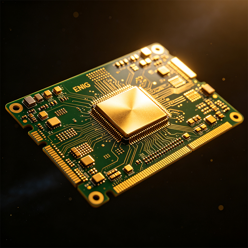
Why Is ENIG So Popular?
ENIG offers several advantages that make it the go‑to surface finish for many applications:
Excellent solderability – The gold layer dissolves instantly into the molten solder, exposing a clean nickel surface that wets easily. You get reliable, shiny solder joints every time.
Extremely flat surface – Unlike HASL (hot air solder leveling) which leaves uneven bumps, ENIG is nearly perfectly flat. That’s crucial for fine‑pitch components (like QFPs, BGAs, and 0.5mm pitch ICs) and for reliable SMT assembly.
Long shelf life – ENIG pads don’t oxidize easily. You can store ENIG‑finished boards for 12–24 months (or even longer) without losing solderability. This is great for manufacturers who need to hold inventory.
Good for wire bonding – The nickel layer is hard enough for aluminum or gold wire bonding (though ENIG is not the best for gold wire bonding – ENEPIG is better).
Excellent corrosion resistance – The nickel‑gold sandwich protects the copper from humidity, salt, and other contaminants.
Good for edge connectors and contact pads – The gold surface provides low and stable contact resistance for sliding or plug‑in connectors (like USB ports, card slots, or gold fingers).
How Does ENIG Compare to Other Surface Finishes?
Here’s a quick comparison with the most common alternatives:
| Finish | Solderability | Flatness | Shelf Life | Cost | Best For |
|---|---|---|---|---|---|
| ENIG | Excellent | Excellent | 12+ months | Medium‑high | Fine‑pitch SMT, BGA, wire bonding, edge connectors |
| HASL (lead‑free) | Good | Poor (uneven) | ~12 months | Low | Low‑cost, through‑hole heavy boards |
| Immersion Silver | Excellent | Very good | 6–12 months | Medium | High‑frequency, tight tolerances |
| OSP | Good (after cleaning) | Excellent | 3–6 months | Very low | High‑volume, short assembly window |
| ENEPIG | Excellent | Excellent | 12+ months | High | Wire bonding, very fine pitch, high reliability |
What Are the Disadvantages of ENIG?
No finish is perfect. ENIG has a few known issues:
Higher cost – ENIG is more expensive than HASL or OSP because of the gold and the complex chemical process. However, it’s cheaper than ENEPIG.
Black pad (a rare defect) – If the nickel layer is poorly controlled or over‑etched during the gold immersion step, the nickel can become darkened, brittle, and non‑wettable. This is called “black pad.” It’s rare with modern processes, but it’s a known risk.
Gold embrittlement – If the gold layer is too thick (>0.2 microns), it can cause weak, brittle solder joints. That’s why ENIG gold is kept very thin.
Not for all wire bonding – Gold wire bonding to ENIG can be problematic; ENEPIG is preferred for that application.
Possible signal loss at very high frequencies – At frequencies above 10 GHz, the nickel layer can cause some signal loss due to its magnetic properties. For millimeter‑wave applications, other finishes (like immersion silver or direct gold) may be better.
Where Is ENIG Used?
You’ll find ENIG in products that demand high reliability, fine‑pitch components, or long storage life:
Smartphones and tablets – The main board uses ENIG for fine‑pitch BGAs and connection pads.
Medical devices – Implantable devices, patient monitors, and diagnostic equipment require long‑term reliability and corrosion resistance.
Automotive electronics – ECU, ADAS sensors, and infotainment systems often specify ENIG.
Aerospace and defense – High‑reliability boards (avionics, radar, communication) use ENIG for its stability.
Industrial controls – PLCs, drives, and HMIs where boards may sit in inventory for months before assembly.
Keyboards and consumer electronics – Many custom mechanical keyboards use ENIG for its flatness and gold appearance.
What About Flexible and Rigid‑Flex PCBs?
ENIG works beautifully on flexible circuits (polyimide base) and rigid‑flex boards. The process is the same, with one caution: flexible materials can be sensitive to the chemical baths, so the parameters must be carefully controlled. ENIG is actually the preferred finish for many flex circuits because it provides a flat, solderable surface that doesn’t crack when the board bends – unlike HASL, which can be uneven and brittle.
ENIG vs. ENEPIG – What’s the Difference?
ENEPIG (Electroless Nickel Electroless Palladium Immersion Gold) adds a layer of palladium between the nickel and the gold. The palladium layer prevents the nickel from corroding and eliminates the “black pad” risk. ENEPIG is more expensive but is the go‑to finish for high‑reliability wire bonding and very fine‑pitch BGAs. For most applications, ENIG is sufficient.
Can You Solder on ENIG After Long Storage?
Yes. One of ENIG’s biggest advantages is its long shelf life. Even after 12–24 months (if stored properly in a sealed bag with desiccant), ENIG pads remain solderable. You may need to use a slightly more active flux if the board is very old, but generally, it solders like new.
How to Specify ENIG on Your PCB Order
When ordering PCBs, you’ll see ENIG listed as a surface finish option. Here’s what to specify:
ENIG – Standard thickness: 0.05–0.1 microns gold over 3–5 microns nickel.
Thick ENIG – For applications requiring heavy gold (e.g., edge connectors that will be plugged/unplugged often). Specify 0.2–0.4 microns gold.
ENEPIG – If you need palladium (for wire bonding or extreme reliability).
A Real‑World Example: Why an Industrial Customer Switched to ENIG
A customer was manufacturing industrial control boards using lead‑free HASL. The HASL gave an uneven surface, causing placement problems for a 0.5mm pitch QFP chip. They also had storage issues – boards left in the warehouse for three months were hard to solder. They switched to ENIG. The flat surface solved the placement problem, and the long shelf life eliminated the storage worry. The slightly higher cost was worth it.
Final Answer – What Is ENIG Plating?
ENIG (Electroless Nickel Immersion Gold) is a two‑layer surface finish for PCBs: a nickel layer (3–6µm) deposited electrolessly on the copper, followed by a very thin gold layer (0.05–0.2µm) by immersion. It provides a flat, solderable, corrosion‑resistant surface with a long shelf life. ENIG is ideal for fine‑pitch SMT components, BGAs, edge connectors, and high‑reliability applications. It’s more expensive than HASL or OSP but offers superior performance.

Kaboer manufacturing PCBs since 2009. Professional technology and high-precision Printed Circuit Boards involved in Medical, IOT, UAV, Aviation, Automotive, Aerospace, Industrial Control, Artificial Intelligence, Consumer Electronics etc..


 English



 Wechat
 +86 13670210335
 +86 13670210335
 E-mail