
Date: 2026-07-18
You're designing an electronic product. Maybe an industrial controller, an automotive ECU, a medical device, or a telecom base station. You don't need a board that "just works" — you need a board that survives in harsh environments for a decade or more.
Industrial PCB production isn't lab prototyping or small-batch trial runs. It's scalable, standardized, high-reliability circuit board manufacturing for automotive, aerospace, medical, and industrial automation. It demands not just "making it work," but every board must withstand temperature shock, vibration, moisture, and the test of time.
In this guide, I'll explain what industrial PCB production is, why it's different from ordinary boards, how the process works, and how to choose the right manufacturing partner. Plain English, no fluff.
Industrial PCB production is the large-scale manufacturing of PCBs that meet industrial-grade reliability standards under tightly controlled process conditions.
The key differences from prototyping or consumer-grade PCB production:
Repeatability: Every batch must perform consistently — no batch-to-batch variation
Precision: Line widths, hole sizes, and impedance tolerances are far tighter than consumer-grade
Traceability: Every board's materials, process parameters, and test results must be traceable
International standards compliance: Must meet IPC, UL, RoHS, and other global standards
An industrial-grade PCB may need to work for 10-20 years, installed in equipment that's rarely opened for repair. So unlike consumer electronics that are "replace when broken," industrial boards must be reliable before they leave the factory.
The global PCB market is undergoing structural growth. According to Prismark, the global PCB market is expected to reach $95.78 billion in 2026**, up **12.5% year-over-year**. Other forecasts project **$105.2 billion in 2026, with a 13.9% growth rate.
The growth is driven by three major forces:
AI Servers: Global AI server shipments are expected to exceed 2 million units in 2026, driving high-end PCB demand growth of over 110% year-over-year. A single AI server's PCB value is nearly 10 times that of a standard server.
Automotive Electronics: EVs, ADAS (Advanced Driver-Assistance Systems), and smart cockpits are driving automotive electronics architecture toward domain control and centralized computing. Demand for multi-layer boards, high-end HDI, and high-frequency boards continues to rise.
Communications Infrastructure: 5G base stations, high-speed switches, optical modules — all require low-loss, high-reliability PCBs.
The global PCB assembly market was valued at $97.88 billion in 2025** and is projected to reach **$103.37 billion in 2026, with a 6.12% CAGR. Industrial PCBs account for an increasing share of this market.
| Feature | Industrial PCB Production | Standard PCB Production |
|---|---|---|
| Target lifespan | 10-20 years | 2-5 years |
| Operating environment | High heat, humidity, vibration | Mild conditions |
| Material grade | High-Tg FR4, Rogers, Polyimide | Standard FR4 |
| Tolerance requirements | ±5-10% (impedance, hole size) | ±20% |
| Quality standard | IPC Class 2/3 | IPC Class 1/2 |
| Traceability | Board-level traceability | Batch-level traceability |
| Testing coverage | 100% electrical + reliability testing | Sampling |
Industrial PCB production isn't just "turning designs into boards." It's a complex system involving materials science, chemical engineering, precision machining, automation, and quality management.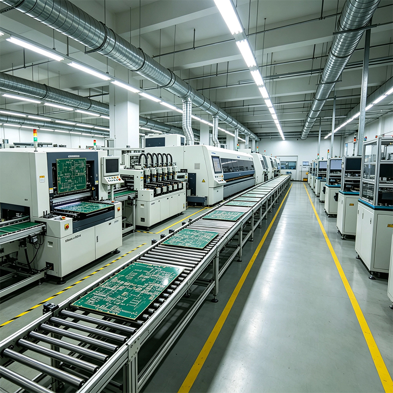
Step 1: Design Data Preparation and Engineering Review
Industrial PCB production starts with design file review. Customers provide Gerber files, ODB++, IPC-2581, drill files, netlists, and fabrication drawings. These files define board outline, copper layers, solder mask openings, silkscreen, drill locations, impedance requirements, and stackup.
A DFM (Design for Manufacturing) check is performed — trace width, spacing, annular rings, material selection. Industrial PCB DFM is far more stringent than consumer-grade — an issue that might "pass" in consumer electronics could cause a field failure in industrial applications.
Step 2: Material Selection
Material choice determines electrical, mechanical, and thermal performance. Common industrial PCB materials include:
High-Tg FR4: Heat-resistant, suitable for lead-free soldering and high-temperature environments
Polyimide: Core material for flexible and rigid-flex boards
Rogers/PTFE: High-frequency, high-speed signal applications
Metal-core substrates: High-power LED and power electronics
Step 3: Inner Layer Imaging and Pattern Transfer
For multi-layer boards, each inner copper layer is patterned independently. Photosensitive material is applied to copper-clad boards, and the circuit pattern is exposed using laser photoplotters or direct imaging systems. Unwanted copper is etched away. Industrial PCB line-width tolerance is controlled to within ±10% — far tighter than consumer-grade.
Step 4: Lamination
Inner layers, prepreg, and copper foil are stacked and pressed under high heat and pressure. Interlayer alignment precision directly determines yield — misalignment beyond 0.05mm means vias may miss pads.
Step 5: Drilling and Plating
Holes are drilled — mechanical drilling for through-holes, laser drilling for blind and microvias. Copper is deposited on hole walls to connect different layers.
Step 6: Outer Layer and Solder Mask
Outer layer circuits are produced, and solder mask (green coating) is applied to protect traces and prevent shorts. Industrial PCB solder mask thickness and adhesion requirements are far more demanding than consumer-grade.
Step 7: Surface Finish
Surface finishes — ENIG (gold), HASL (tin), OSP — are applied to pads. ENIG is the preferred choice for industrial applications — flat, oxidation-resistant, and long shelf life.
Step 8: Electrical Testing and QA
100% electrical testing — opens, shorts, impedance. Industrial PCBs also require reliability testing: thermal cycling, thermal shock, vibration, and high-humidity testing.
Industrial PCB performance depends heavily on material selection:
FR4 (High-Tg): The most common substrate. Standard FR4 Tg is 130-140°C; high-Tg FR4 reaches 170-180°C. Lead-free soldering runs hotter — high-Tg FR4 is the entry requirement for industrial applications.
Copper Foil: The conductive layer forming traces. Industrial applications commonly use 1oz to 3oz heavy copper for high current.
Solder Mask: Protects traces and prevents shorts. Industrial PCBs typically use LPI (Liquid Photoimageable) solder mask — high precision and strong adhesion.
Surface Finish: ENIG (gold) is the preferred choice for industrial applications — flat, oxidation-resistant, and long shelf life.
Current challenges:
Rising material costs: Copper foil, resin, and fiberglass prices are volatile
Tighter precision requirements: AI servers and 5G demand ever-tighter line widths and impedance
Lead time pressure: Customers want boards faster, but industrial PCB production cycles are inherently longer than standard boards
Future trends:
AI-driven manufacturing: IPC-2581 is becoming the standard data format for digital manufacturing, enabling AI-driven PCB production
HDI becoming mainstream: The HDI PCB market was valued at $19.59 billion in 2025** and is projected to reach **$34.23 billion by 2032
Flex and rigid-flex growth: The global flexible PCB market was $23.3 billion in 2025**, projected to reach **$41.7 billion by 2030
We are not a standard rigid-only PCB shop. We are a one-stop manufacturer that designs and makes flexible PCBs, rigid-flex boards, HDI high-frequency boards, and then does full PCBA.
All in-house: PCB fabrication, SMT, DIP, and testing under one roof. No handoffs — every step under our control.
High-reliability material experience: High-Tg FR4, Rogers, PTFE, Polyimide — we've done them all for automotive, medical, and telecom applications.
High-precision manufacturing: Minimum trace/space 0.05mm, minimum laser blind via 0.075mm. Supports 1-order to any-layer HDI, up to 20+ layers.
IPC-compliant: Fabrication and inspection to IPC-6012, IPC-A-610, and IPC-J-STD-001 — Class 2 and 3.
Full testing capability: SPI, AOI, X-Ray, ICT, FCT — every industrial board goes through full testing before shipping.
Free DFM review: Send your design files, get a DFM report within 24 hours — including material recommendations, manufacturability assessment, and potential issue warnings.
Three simple steps:
Send your files: Gerbers, BOM, stackup and impedance requirements, target application.
We review and quote: Within 24 hours, you'll receive a DFM report, material recommendations, and sample/volume pricing.
Sample, then scale: We build samples. You test functionality and reliability. Then we move to volume.
Industrial PCBs aren't "more expensive regular boards" — they're built to solve problems that regular boards can't handle. The global PCB market is set to exceed $100 billion in 2026, with AI and automotive driving unprecedented growth.
If you're looking for a PCB manufacturer that truly understands industrial-grade reliability, high-layer-count boards, HDI, and rigid-flex, send us your requirements. We won't push a contract — we'll first run a free DFM review and material recommendation, and let our expertise speak.
When you contact us, please include:
Product type and application (industrial, automotive, medical, telecom, etc.)
Estimated layer count and whether flex or high-frequency is required
Estimated annual quantity (samples, small batch, or mass production)
We'll give you an honest answer — what we can do, what we can't, and how to modify your design to make it work.

Kaboer manufacturing PCBs since 2009. Professional technology and high-precision Printed Circuit Boards involved in Medical, IOT, UAV, Aviation, Automotive, Aerospace, Industrial Control, Artificial Intelligence, Consumer Electronics etc..


 English



 Wechat
 +86 13670210335
 +86 13670210335
 E-mail