Manufacturing Process of Flexible Printed Circuit Boards (FPCB)
Date: 2025-12-02
The manufacturing process of Flexible Printed Circuit Boards (FPCB) is relatively complex, involving more than a dozen procedures. The manufacturing difficulty varies with the complexity of the board type: approximately 15-20 procedures for single-sided boards, 18-22 for double-sided boards, and 22-30 for multi-layer boards. Below are the core mandatory procedures:
-
Material Preparation
-
Select Polyimide (PI) or Polyester (PET) base film
-
Choose copper foil (Electrodeposited Copper/EDCu or Rolled Annealed Copper/RACu)
-
Prepare auxiliary materials (adhesive, cover film, etc.)
-
Base Film Pretreatment
-
Plasma/corona treatment: Enhance surface adhesion (surface tension ≥40mN/m)
-
Cleaning and degreasing to ensure no impurities
-
Copper Lamination
-
Bond copper foil to base film via thermal compression (120-160℃, 1-2MPa)
-
Peel strength ≥0.5N/mm to prevent copper foil detachment
-
Photolithography (Pattern Transfer)
-
Apply photosensitive film → Expose → Develop → Form circuit patterns
-
Alignment accuracy ≤±2μm to ensure circuit precision
-
Etching
-
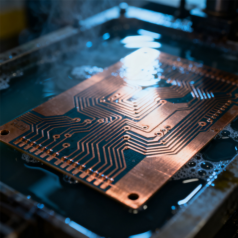
Remove unprotected copper foil using acidic copper chloride etchant
-
Control undercut ratio ≤1:1 to guarantee line width accuracy
-
Drilling/Punching

-
Via Metallization
-
Chemical copper deposition + electroplating: Form a conductive layer on hole walls to achieve interlayer connection
-
Cover Film Lamination
-
Window opening → Alignment → Thermal compression (160-180℃) → Curing
-
Protect circuits from moisture and provide insulation
-
Surface Finish
-
Electroless Nickel Immersion Gold (ENIG)/Immersion Tin/Organic Solderability Preservative (OSP)
-
Prevent copper oxidation and improve solderability
-
Forming Process
-
Laser cutting/die cutting: Precisely trim to the final shape
-
Electrical Testing
-
Continuity test + insulation test: Ensure normal circuit functionality
-
Visual Inspection
-
AOI (Automatic Optical Inspection) + manual inspection: Detect defects
-
Packaging & Shipping
-
Anti-static packaging to protect finished products
The above procedures are mandatory for FPCB manufacturing. Additional procedures are required when classified by board type:
Material Preparation → Base Film Pretreatment → Copper Lamination → Photolithography (Film Lamination → Exposure → Development) → Etching → Stripping → Drilling → Surface Finish → Cover Film Lamination (Alignment → Thermal Compression → Curing) → Silkscreen Printing → Forming → Electrical Testing → Visual Inspection → Packaging
Add the following to single-sided FPCB procedures:
-
Via Metallization (Black Hole/Chemical Copper Deposition → Electroplating)
-
Second Pattern Transfer and Etching
Add the following to double-sided FPCB procedures:
-
Inner Layer Circuit Fabrication (for each layer)
-
Lamination (Brown Oxidation → Pre-stacking → Compression Bonding)
-
Additional Via Processing and Interlayer Alignment
For special requirements, the following flexibility enhancement procedures can be added:
-
Reinforcement
-
Attach rigid materials (PI/FR-4) to stress-bearing areas (e.g., connectors) to prevent bending fracture
-
Ultra-thin PI film (≤25μm) for cover film to ensure bending performance
-
Reliability Testing (Optional but Critical)
-
Bending Test: Simulate real-world bending (≥100,000 cycles)
-
Thermal Shock Test: Verify stability under extreme temperatures (-55℃~125℃)
FPCB manufacturing is a sophisticated systematic project. From material selection to finished products, each procedure directly impacts the performance, reliability, and service life of the FPCB. In particular, process control over flexibility, precision, and connection reliability is the core technology that distinguishes FPCBs from rigid PCBs.