
Date: 2026-05-25
Imagine you're carving a piece of wood. You want to remove just enough material to leave your design clean and crisp. But you go a little too deep, and suddenly the lines become too thin, some details disappear, and the whole piece looks ragged. That’s essentially what overetching does to a circuit board.
Overetching is one of the most common defects in PCB manufacturing. It happens when the chemical etching process removes more copper than intended, thinning traces, narrowing pads, and sometimes even erasing whole features. Let’s dive into what overetching is, why it happens, how to spot it, and what you can do to prevent it.
What Is Etching and How Does It Work?
Before we talk about overetching, let's quickly cover what normal etching does.
A circuit board starts as a copper‑clad board – a sheet of insulating material (like FR4) with a thin layer of copper foil on one or both sides. To create the copper traces and pads, manufacturers apply a photoresist – a light‑sensitive material that protects the areas that should remain copper. The board is exposed to UV light through a film that has the circuit pattern. The areas that get light harden; the unexposed areas stay soft. Then the board goes through an etching solution (usually an acidic or alkaline chemical) that dissolves the unprotected copper. Finally, the hardened photoresist is stripped away, leaving the copper traces.
In a perfect world, the etchant would remove exactly the unwanted copper and stop precisely at the edge of the resist. In reality, the chemical doesn’t stop perfectly. It also eats a little bit sideways, under the resist. That sideways attack is called undercutting. When the undercutting is excessive, the copper traces become narrower than intended. That’s overetching.
What Does Overetching Look Like?
You can spot overetching with a magnifying glass or a microscope. Here are the telltale signs:
Thinner traces – The copper lines look skinnier than the design specifies. Instead of a nice, straight line with parallel edges, the trace narrows or becomes wavy.
Pitted or rough surfaces – The copper surface looks pockmarked or uneven.
Narrowed or missing pads – The annular rings around via holes become thinner, and sometimes the pad disappears entirely.
Broken traces – In severe cases, the trace is completely etched away at some points, creating an open circuit.
Loss of fine features – Fine details like small logos, text, or identification marks can vanish.
One specific sign of overetching that designers and manufacturers often notice is damage to the logo or text printed on the copper layer. For example, if a manufacturer has a logo on the board as part of the copper etch (not just silkscreen), overetching can make the logo unrecognizable – lines become too thin, sharp corners round off, and small gaps close up.
What Causes Overetching?
Several factors can lead to overetching:
Etching time too long – The board stays in the etching solution longer than necessary. That gives the chemical more time to eat away the copper.
Solution too hot or too concentrated – Higher temperature or stronger concentration accelerates the reaction, making it harder to stop at the right moment.
Solution too old or contaminated – Old or dirty etchant can behave unpredictably, sometimes etching unevenly.
Insufficient agitation – If the solution isn’t moving enough, fresh etchant may not reach all areas uniformly, leading to overetching in some spots while underetching in others.
Resist too thin or damaged – The photoresist layer protects the copper. If it’s too thin or has pinholes, the etchant can attack through it, causing overetching in localized areas.
Incorrect photoresist selection – Some resists are designed for specific etchants. Using the wrong combination can cause poor adhesion or excessive undercutting.
Overetching vs. Underetching – What’s the Difference?
Understanding the contrast helps clarify the concept.
| Defect | What Happens | Result |
|---|---|---|
| Overetching | Too much copper removed | Thin traces, narrow pads, open circuits |
| Underetching | Not enough copper removed | Copper residue between traces (short circuits) |
Overetching leaves your traces anorexic; underetching leaves unwanted bridges between them. Both are bad, but they have opposite causes and visual appearances.
How Overetching Affects Different Types of PCBs
Standard rigid boards – Overetching reduces the cross‑section of the copper traces, which increases electrical resistance. For high‑current traces, this can cause overheating or voltage drop. For fine‑pitch surface‑mount pads, overetching can reduce the pad size so much that components don’t solder properly.
Flexible PCBs – Flex circuits (made of polyimide) are even more sensitive to overetching. The copper is often thinner to begin with (typically 12–35µm instead of 35–70µm), so there’s less margin for error. Overetching can quickly lead to broken traces, especially in dynamic flex areas where the board bends repeatedly.
HDI and high‑frequency boards – These boards have very fine traces (sometimes 0.05mm or less). Overetching is a major risk because even a tiny amount of extra copper removal can destroy a trace or change the impedance, messing up signal integrity.
Rigid‑flex boards – The transition zones between rigid and flexible sections are already stress points. Overetching can weaken traces there, leading to cracks during bending.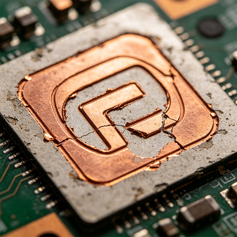
How to Detect Overetching
Manufacturers use several methods to catch overetching before the boards ship:
Visual inspection – Under magnification, operators can see thinning traces, narrow pads, or damaged logos.
Automated Optical Inspection (AOI) – High‑resolution cameras scan the board and compare it to the original design file. AOI can detect trace width variations that are too small for the human eye.
Electrical testing – Flying probe or bed‑of‑nails testers check for open circuits (broken traces) caused by overetching.
Cross‑sectioning – For critical boards, a small sample is cut, mounted, and polished to measure the exact trace width and undercut under a microscope.
Real‑World Example: The Faded Logo
A PCB manufacturer produced a batch of boards for a customer that had a small copper logo etched into the top layer. When the customer received the boards, the logo looked blurry and incomplete – some letters were almost missing. The manufacturer traced the problem to overetching caused by an old etching bath that had been running too long without replenishment. The etchant was overly aggressive, attacking the fine details of the logo and thinning the surrounding traces. The batch was scrapped, and the manufacturer replaced the etching solution and adjusted the process time.
How to Prevent Overetching
For PCB manufacturers, prevention is a matter of process control:
Monitor etchant parameters – Regularly test the concentration, temperature, and pH of the etching solution. Replenish or replace the bath as needed.
Optimize etch time – Use the shortest time that reliably removes the unwanted copper. Over‑etching for safety is not safe – it causes defects.
Use high‑quality photoresist – A uniform, pinhole‑free resist layer resists undercutting better.
Maintain proper agitation – Spray etching or ultrasonic agitation ensures fresh etchant reaches all surfaces evenly, preventing localized overetching.
Implement statistical process control (SPC) – Track key parameters over time and set alarms when they drift outside acceptable limits.
Run test coupons – Small test patterns with fine features can be etched alongside production boards to monitor the process.
What to Do If You Receive Overetched Boards
If you’re a customer who receives PCBs with overetched traces or a damaged logo, here’s what you can do:
Check your design files – Make sure the traces and features are designed with adequate width to allow for normal etching tolerances. For example, if the manufacturer’s process can hold ±0.02mm, don’t design traces at the absolute minimum.
Discuss with your manufacturer – Provide photos or measurements showing the defect. A good manufacturer will investigate and offer a solution – rework (if possible) or replacement.
Consider electrical testing – Even if traces look thin, they might still pass electrical test. A flying probe test can confirm whether the board is functional despite the cosmetic defect.
Final Answer – What Is Overetching in PCB Manufacturing?
Overetching occurs when the chemical etching process removes more copper than intended, resulting in thinner traces, narrowed pads, and sometimes missing features like logos. It’s caused by excessive etch time, incorrect solution parameters, or poor process control. Overetching can lead to open circuits, impedance mismatches, and reliability issues, especially on flexible, HDI, and high‑frequency boards.
Manufacturers prevent overetching by carefully controlling the etching parameters – temperature, concentration, time, and agitation. If you receive overetched boards, document the defect and work with your manufacturer to correct the process.
Next time you see a PCB with copper traces that look unusually skinny or a logo that’s barely recognizable, you’ll know: that’s overetching, and it’s a sign that the etching process wasn’t quite right.

Kaboer manufacturing PCBs since 2009. Professional technology and high-precision Printed Circuit Boards involved in Medical, IOT, UAV, Aviation, Automotive, Aerospace, Industrial Control, Artificial Intelligence, Consumer Electronics etc..


 English



 Wechat
 +86 13670210335
 +86 13670210335
 E-mail