Date: 2026-01-08
PCB manufacturing and assembly are two closely linked yet distinct professional stages. Together, they transform design schematics into functional hardware products.
Put simply: PCB manufacturing creates the bare board, while PCB assembly mounts all the electronic components onto it. Understanding this distinction is helpful for project management.
This is the production starting point. Factories create bare printed circuit boards based on design files (typically Gerber files).
Key steps include:
Substrate Preparation: Usually starting with a copper-clad insulating laminate (like FR-4)
Pattern Transfer: Using photolithography or printing to transfer the circuit pattern onto the copper foil
Etching: Using chemicals to remove unwanted copper, leaving behind the designed circuit traces
Drilling & Plating: Drilling component holes and vias, then plating the hole walls to make them conductive
Solder Mask & Silkscreen: Applying a protective coating (usually green) and printing identification text
The focus here is on precision and consistency—trace widths, hole sizes, and layer alignment must be tightly controlled to ensure the circuit performs as designed.
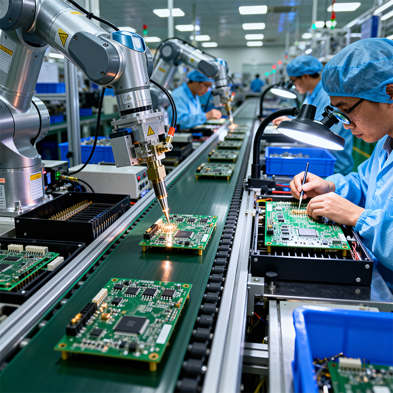
Once the bare PCBs are fabricated, the assembly process begins. This is what's commonly called PCBA (Printed Circuit Board Assembly).
Core processes include:
Solder Paste Printing: Precisely printing solder paste onto pads through a stencil
Component Placement: SMT equipment rapidly places tiny components in their designated positions
Reflow Soldering: Passing the board through a temperature-controlled oven to melt the solder paste, forming solid electrical connections
Through-Hole & Wave Soldering: Installing and soldering any through-hole components
Cleaning & Inspection: Cleaning flux residue and performing optical and electrical inspections
The focus here is on process control—everything from solder paste quality and placement accuracy to soldering temperature directly impacts the final product's reliability.
In practical projects, having the same partner handle both manufacturing and assembly typically brings several tangible benefits:
Higher Communication Efficiency
Design and process issues can be coordinated and resolved internally, avoiding back-and-forth between two separate suppliers.
More Complete Quality Control
Clear accountability for quality spans the entire process from material selection to final assembly, enabling more direct problem tracing.
Tighter Scheduling
Seamless handoffs between processes reduce logistics and waiting time, leading to more predictable overall lead times.
More Transparent Cost Control
Combined quotes are often clearer than sourcing separately, and they eliminate markups from intermediate steps.
At Kaboer's factory in Shenzhen, these two stages operate within the same management system. We observe that when manufacturing and assembly are seamlessly integrated, the speed from design to prototype can increase noticeably. Furthermore, issues identified early in production can be fed back more quickly into manufacturing process adjustments.
When looking for PCB manufacturing and assembly services, it's wise to consider the following:
Technical Capability Match
Does your product involve special processes? For example, high-frequency boards require different manufacturing techniques, while densely packed components demand high-precision assembly equipment.
Production Scale and Flexibility
Can the partner adapt to different needs, from rapid prototyping to volume production? How flexible is their line changeover?
Quality Management System
Do they have a systematic quality control process? Are the control points and inspection methods for critical steps well-established?
Supply Chain Stability
Especially in the current environment of component supply fluctuations, supplier management capability is particularly important.
Communication and Transparency
Can they provide clear production progress updates? How quickly do they respond when technical issues arise?
At its core, PCB manufacturing and assembly is a precise process of translating abstract designs into physical objects. In this process, design intent must be accurately understood and realized through professional craftsmanship.
For teams that prefer to focus on product design and market development, finding a reliable manufacturing and assembly partner means entrusting complex production management to specialists, freeing up energy to build core competencies.
In electronics hardware, good design requires equally good manufacturing to realize its value. Understanding the complete manufacturing and assembly process helps in making more informed planning decisions early in product development.
Kaboer manufacturing PCBs since 2009. Professional technology and high-precision Printed Circuit Boards involved in Medical, IOT, UAV, Aviation, Automotive, Aerospace, Industrial Control, Artificial Intelligence, Consumer Electronics etc..