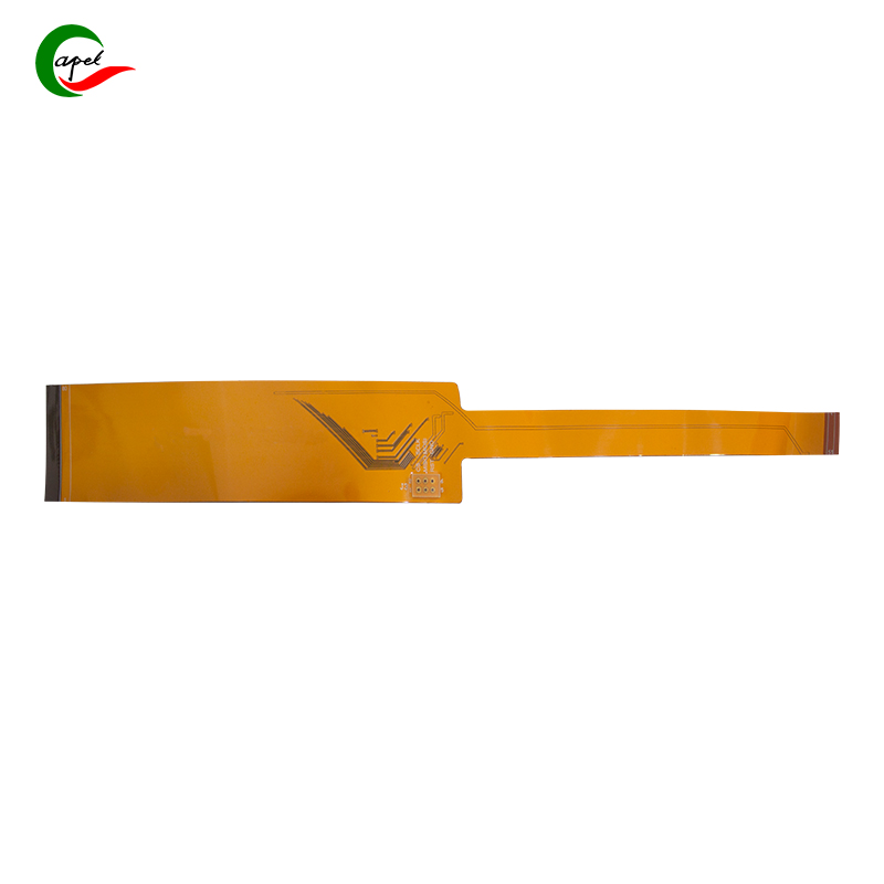
The demand for smaller, more powerful, and flexible electronic devices—from foldable smartphones to medical wearables—has sparked innovation at the intersection of flexible printed circuits (FPCs) and high-density interconnect (HDI) technology. A key question emerges: Can flexible PCBs integrate HDI technology? The answer is a resounding yes—and this combination is revolutionizing how electronics are designed and deployed.
Flexible PCBs (FPCs) use bendable substrates like polyimide (PI) to withstand repeated folding or twisting, while HDI technology enables dense circuitry with microvias (≤0.15mm) and fine line/space (L/S) ratios (≤3mil/3mil). Together, they create “flexible HDI PCBs”—a hybrid solution that merges flexibility with high-density performance.
- Core Components: Flexible HDI PCBs typically use PI as the base substrate (for flexibility) and integrate HDI features like microvias, stacked vias, and fine traces.
- Manufacturing Adaptations: Specialized processes—such as laser drilling for microvias in thin PI layers and precision lamination—ensure HDI features don’t compromise the FPC’s bendability.
This hybrid technology offers unique benefits that neither flexible PCBs nor HDI alone can match:
- Miniaturization Without Sacrificing Flexibility: HDI’s microvias and fine traces allow more components (e.g., sensors, chips) to be packed into flexible FPCs, enabling ultra-compact designs for wearables and IoT devices.
- Enhanced Signal Performance: Shorter signal paths in HDI reduce crosstalk and latency, critical for high-speed applications like 5G modules in foldable phones.
- Design Versatility: Flexible HDI PCBs conform to curved or irregular surfaces (e.g., automotive dashboards, medical implants) while supporting complex circuitry.
- Weight Reduction: Dense HDI layouts eliminate the need for bulky connectors, making devices lighter—ideal for aerospace and portable electronics.
Flexible HDI PCBs are transforming industries where space, flexibility, and performance are equally critical:
- Consumer Electronics: Foldable smartphones and tablets use flexible HDI to connect hinges and displays, supporting high-resolution screens and 5G connectivity in a foldable form.
- Medical Devices: Wearable health monitors (e.g., ECG patches) and implantable devices (e.g., pacemakers) rely on flexible HDI to fit the body’s contours while housing dense sensors and wireless transmitters.
- Automotive Systems: They integrate into curved infotainment screens and ADAS (Advanced Driver-Assistance Systems), enabling compact, high-performance circuitry in limited cabin space.
- Aerospace: Lightweight, flexible HDI PCBs reduce aircraft weight while supporting avionics with high-frequency communication needs.
While promising, flexible HDI technology faces unique hurdles:
- Manufacturing Complexity: Laser drilling microvias in thin PI substrates requires extreme precision to avoid damaging the flexible layer. This increases production costs compared to standard FPCs.
- Mechanical Stress: Repeated bending can strain microvias and fine traces, leading to fatigue or failure. Engineers must balance density with flexibility, often using thicker copper in critical areas.
- Material Compatibility: Adhesives and laminates used in HDI must bond well with PI without stiffening the FPC excessively.
- Testing Rigor: Traditional inspection tools may struggle to detect flaws in tiny microvias on flexible surfaces, requiring advanced AOI (Automated Optical Inspection) systems.
As demand grows, innovations are addressing these challenges:
- Advanced Materials: New PI blends with higher thermal resistance and flexibility are being developed to support denser HDI layouts.
- 3D Integration: Flexible HDI PCBs are increasingly combined with rigid HDI sections (rigid-flex designs) to balance component mounting stability with bendability.
- AI-Driven Design: Software tools optimize trace routing and via placement to minimize stress during bending, improving durability.
Flexible PCBs can indeed leverage HDI technology, and their combination is a game-changer for compact, high-performance electronics. While manufacturing complexity and cost remain considerations, the benefits—miniaturization, design versatility, and enhanced signal performance—make flexible HDI PCBs indispensable for next-generation devices. As technology advances, we can expect even more innovative applications, solidifying this hybrid solution as a cornerstone of modern electronics design.
Founded in 2009, our company has deep roots in the production of various circuit boards. We are dedicated to laying a solid electronic foundation and providing key support for the development of diverse industries.
Whether you are engaged in electronic manufacturing, smart device R&D, or any other field with circuit board needs, feel free to reach out to us via email at sales06@kbefpc.com. We look forward to addressing your inquiries, customizing solutions, and sincerely invite partners from all sectors to consult and collaborate, exploring new possibilities in the industry together.
