Date: 2025-07-25
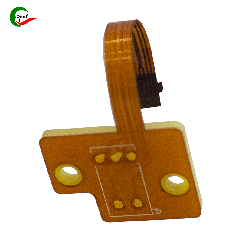
Double-sided flexible circuit boards (double-sided FPCs) are core components of sophisticated electronic devices, designed and produced with a focus on flexibility and functionality. Below is an explanation of their core features.
Construction: Double-sided Wiring for Enhanced Connectivity and Protection
Double-sided FPCs are built on the "insulating base film + double-sided conductive graphics" structure: A flexible insulating base film (e.g., PI material) has an etched layer of conductive wiring on both sides. This design significantly increases wiring density per unit area, enabling a more compact circuit layout suitable for equipment miniaturization.
To connect the wiring on both sides, metallized holes play a key role—acting as "conductive bridges" through the base film. They link the two sides of the wiring via metal plating on the hole walls, forming a complete pathway while ensuring stable signal transmission during device bending.
The cover film serves as a "protection and indication layer": It not only protects wires from damage but also clearly labels component installation positions to enhance assembly efficiency.
Thickness: Flexible Adaptation to Multiple Scenarios
The thickness of double-sided FPCs can be adjusted based on demand, covering different application scenarios:
Ultra-thin model (0.06MM - 0.1MM): Suitable for thickness-sensitive components such as folding screen hinges and camera modules. High-precision processing is required to guarantee toughness and performance.
Regular model (0.12MM - 0.23MM): Balances performance and cost, widely used in consumer electronics (e.g., TWS headphones, tablet PCs) and industrial modules.
Thickened model (0.3MM): Designed for high-power devices and automotive electronics, capable of carrying higher currents. Production requires attention to the stability of inter-layer bonding.
Production Process: Multi-process Precision Collaboration
The production of double-sided FPCs involves over 20 core processes, with key steps including:
Cutting and drilling: Raw materials are cut and holes are drilled to prepare for subsequent connectivity.
Hole metallization and plating: The PTH process is used to make hole walls conductive, followed by plating to thicken the copper layer and strengthen
wiring conductivity.
Graphics production: After applying dry film, exposure and development are used to define the wiring pattern. Excess copper foil is removed by etching, and the remaining dry film is stripped to reveal the wiring.
Surface and protective treatment: Nickel-gold plating is applied to the surface to enhance abrasion resistance and weldability. A cover film is attached and cured under pressure to strengthen protection.
Post-processing: Identification characters are printed, followed by edge cutting, electrical testing (to detect circuit continuity), punch forming, final inspection, and packaging of qualified products for shipment.
With its flexible structure, adaptable thickness, and precise production process, double-sided FPC continues to support the lightweight and highly integrated development of electronic devices, serving as an important foundation for innovation in the electronics industry.
Established in 2009, our company has deep expertise in the production of various circuit boards, dedicated to building electronic foundations and providing key support for different industries. Whether you are in electronics manufacturing, intelligent equipment research and development, or other industries with circuit board needs, you can communicate with us via email at sales06@kbefpc.com. We look forward to answering your questions, customizing solutions, and sincerely inviting partners from all walks of life to consult and cooperate to explore new industry possibilities.
Kaboer manufacturing PCBs since 2009. Professional technology and high-precision Printed Circuit Boards involved in Medical, IOT, UAV, Aviation, Automotive, Aerospace, Industrial Control, Artificial Intelligence, Consumer Electronics etc..