Date: 2025-12-17
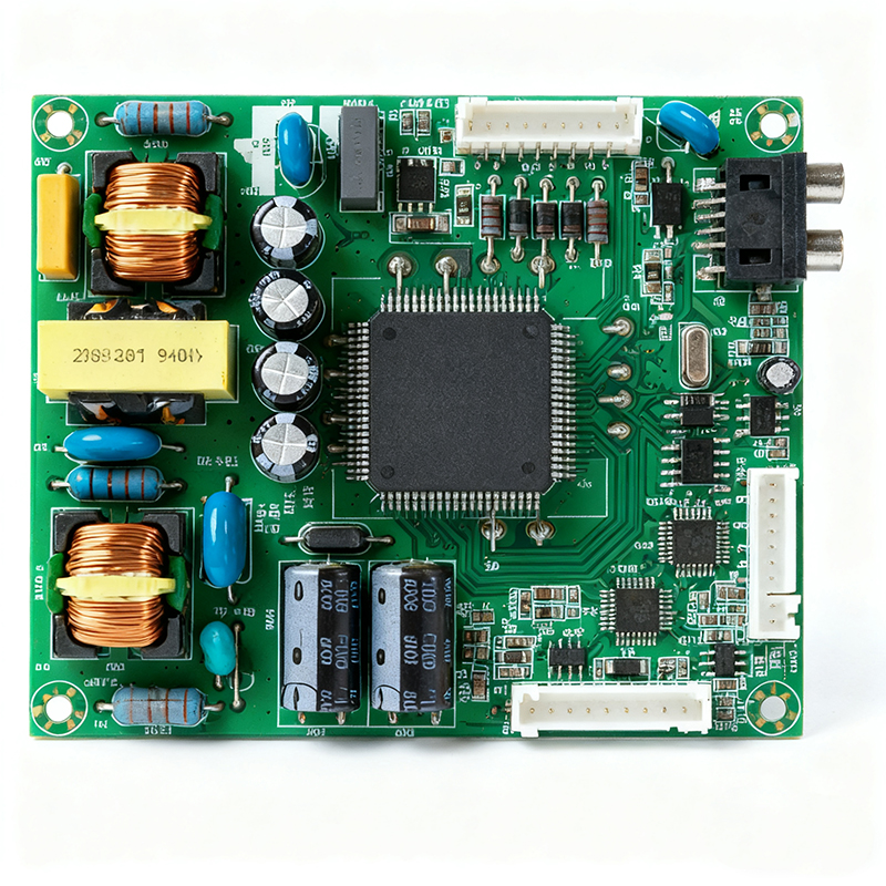
When you think about circuit boards, your mind might first go to the tiny, dense brains inside smartphones or wearables. But what powers the server racks in data centers, the control systems in factories, or the diagnostic screens in medical equipment? Often, it's the large circuit board—an engineering powerhouse that plays a fundamentally different role from its smaller counterparts.
For product designers and manufacturers working on high-end computing, industrial equipment, or large-scale displays, understanding the capabilities and challenges of large-format PCBs is crucial. It's not just a matter of scaling up a design; it's about mastering a distinct discipline in electronics manufacturing.
There's no universal threshold, but in the PCB industry, a board is typically considered "large" when its longest dimension exceeds 18 inches (about 460mm) or when its total area pushes the standard production panel's limits (often 21"x24" or larger).
More than just physical size, what defines these boards is their purpose-driven design. They are built to integrate numerous functions, host high-power components, and manage complex signal integrity across a broad area, often making them the central "motherboard" or backplane of an entire system.
Large circuit boards aren't used in portable devices; they are the foundation for systems where performance, integration, and reliability take precedence over size.
High-Performance Computing & Servers: Backplanes and motherboards that connect dozens of processor cards, memory banks, and networking modules in data centers.
Industrial & Automation Control: Large-format controllers for assembly lines, CNC machines, and power distribution systems that consolidate I/O, processing, and communication on a single, robust platform.
Medical & Diagnostic Imaging: The internal boards for MRI, CT scanners, and ultrasound machines, which require large areas for signal processing arrays and noise isolation.
Telecommunications Infrastructure: Base station units and network switch boards that handle massive data throughput.
Avionics & Defense Systems: Ruggedized control and display units in aircraft and military vehicles.
Large-Format LED Displays & Digital Signage: The specialized driver boards that control vast arrays of LEDs or LCD panels seamlessly.

Designing and producing a reliable large circuit board is a significant technical undertaking. Its advantages come hand-in-hand with specific manufacturing hurdles that not all factories can overcome.
The Value: Why Go Large?
System Integration: A single large board can replace a rack of interconnected smaller boards, reducing points of failure, simplifying cabling, and improving overall system reliability.
Enhanced Thermal & Power Management: The larger surface area allows for better heat dissipation from high-power components (like CPUs and GPUs) and provides more space for robust power plane design.
Signal Integrity for High-Speed Design: Careful layout on a large board can provide dedicated, uninterrupted pathways for critical high-speed signals (like DDR memory buses or PCIe lanes), reducing noise and crosstalk.
The Manufacturing Challenges:
Material Handling & Dimensional Stability: Moving and processing large, thin panels without warping or bowing is difficult. Standard FR-4 can be insufficient; materials with higher Glass Transition Temperature (Tg) and better dimensional stability are often required.
Lamination & Layer Alignment: Achieving perfect alignment (registration) during the multi-layer lamination process is exponentially harder on large panels. Any misalignment can lead to open or short circuits.
Uniform Copper Plating & Etching: Ensuring consistent copper thickness across the entire board surface during electroplating is critical. Inconsistent etching can lead to trace width variations, affecting impedance control.
Precise Drilling & Routing: Drilling thousands of holes with positional accuracy across a large area, and cleanly routing the board outline without splintering, demands high-end, well-maintained equipment.
Testing and Inspection: Electrical testing (flying probe or fixture) takes much longer. Automated Optical Inspection (AOI) systems must have large scan areas and high resolution to reliably detect defects across the entire board.
At Kaboer, located in Shenzhen's manufacturing hub, we recognize that large circuit boards represent a commitment to system-level performance. Our factory is equipped to handle the scale and precision these projects demand.
We address the core challenges through controlled processes, suitable material selection, and equipment capable of large-panel processing. From fabrication to the assembly of large boards—which includes managing solder paste uniformity and precise reflow oven profiling over a large area—we focus on the details that ensure structural integrity and long-term reliability.
For manufacturers designing systems where performance cannot be compromised by size constraints, a partner with proven experience in large-format PCBA is essential. It’s about building not just a board, but a solid, dependable foundation for your most demanding applications.
Kaboer manufacturing PCBs since 2009. Professional technology and high-precision Printed Circuit Boards involved in Medical, IOT, UAV, Aviation, Automotive, Aerospace, Industrial Control, Artificial Intelligence, Consumer Electronics etc..