Date: 2026-01-27
If you look closely at a circuit board, especially a multilayer one, you'll notice lots of little holes. Some are big for component leads, but many are small and often surrounded by a shiny ring. Those are vias. Think of them as the vertical elevators or tiny tunnels that connect the different "floors" (copper layers) of your PCB. Without them, a multilayer board would just be a stack of disconnected layers. Let’s break down what they do and why they’re so crucial in design.
What is a Via, Really?
At its core, a via is a small plated hole that creates an electrical connection between two or more layers of a PCB. It’s not just a plain drilled hole; its inner wall is coated (plated) with a conductive material, usually copper, forming a cylinder that links the traces on different layers.
The Main Types of Vias
Understanding the different types helps you choose the right one for your design.
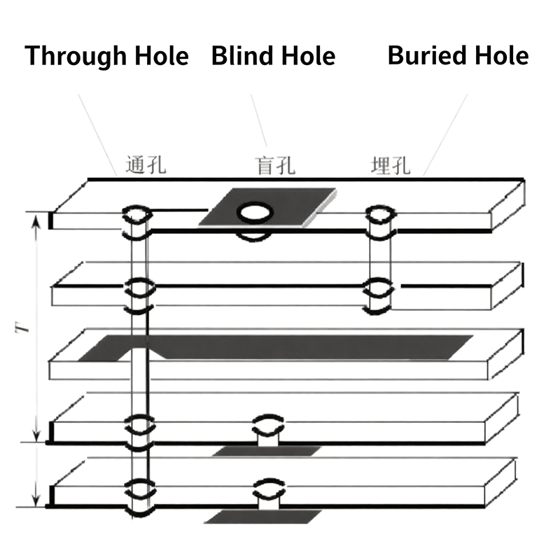
Through-Hole Via:
The Most Common Type. It goes all the way from the top layer to the bottom layer of the board, like a stairwell running through the entire building.
Pros: Easy and cheap to manufacture, mechanically robust.
Cons: Uses space on all layers, which can block routing paths on inner layers.

Blind Via:
Connects an outer layer to one or more inner layers, but does not go all the way through. Imagine an elevator from the lobby (top layer) to the 5th floor (an inner layer), but not to the basement.
Pros: Saves space on layers it doesn’t reach, useful for high-density designs.
Cons: More expensive to make, as it requires precise drilling before lamination.
Buried Via:
Connects two or more inner layers, but is not visible from the outside. Like a service tunnel between the 2nd and 3rd floors, hidden from the lobby or roof.
Pros: Maximizes usable space on outer layers, excellent for ultra-complex, space-constrained designs.
Cons: The most expensive type due to complex manufacturing steps.
Key Design Considerations for Manufacturers
Current Capacity: A via’s ability to carry current depends on the thickness of its copper plating (the barrel). For power paths, you might need multiple vias in parallel to avoid overheating.
Signal Integrity (For High-Speed Designs): Vias introduce a tiny amount of inductance and capacitance, which can disrupt very high-speed signals. Designers use techniques like via stitching (many vias in a row for grounding) and careful placement to manage this.
Manufacturing Cost: More via types and higher densities increase cost. Through-hole vias are the default; blind and buried vias add steps and expense but enable smaller, more advanced boards.
Thermal Path: Vias are fantastic for moving heat! An array of vias under a hot component (called thermal vias) acts like a heat pipe, transferring heat to inner ground planes or the opposite side of the board for dissipation.
Practical Tips for Working with Vias
Don't Overuse: While vias are essential, scattering them everywhere can create routing nightmares and weaken the board structure. Use them purposefully.
Mind the Annular Ring: That shiny copper ring around the hole? It needs to be wide enough to ensure a reliable connection after drilling. Manufacturers have minimum size requirements.
Think About Assembly: If solder can wick into a via during assembly, it might starve a joint. This is called via-in-pad. It can be managed by tenting (covering the via with solder mask) or by specific fill-and-cap processes.
In short, vias are the critical 3D interconnection system within a 2D-looking board. Good via planning is what allows complex, miniaturized, and high-performance electronics to exist. They’re a small feature with a massive impact on functionality, reliability, and cost.
Kaboer manufacturing PCBs since 2009. Professional technology and high-precision Printed Circuit Boards involved in Medical, IOT, UAV, Aviation, Automotive, Aerospace, Industrial Control, Artificial Intelligence, Consumer Electronics etc..