Date: 2026-01-27
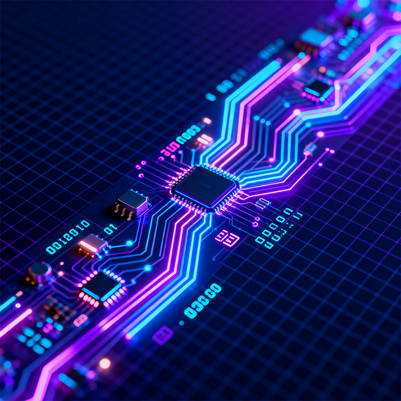
Think about a modern city. What makes everything function? Roads, power lines, and data cables connecting homes, businesses, and services. Now, look inside any electronic device. Those thin, metallic lines you see on a circuit board? Those are the traces. They are the essential roads, highways, and pathways that allow electricity and signals to travel between components. Let’s explore what they are, why they matter, and how they’re designed.
What Exactly Are Traces?
Traces (also called tracks or wiring) are the thin lines of copper foil that are left on the board after the etching process. They are not painted on; they are part of the board's copper layer that is selectively preserved to form connections. They carry electrical current—whether it's power to run a chip or a delicate data signal—from one point to another.
Key Things Every Maker Should Know About Traces
It’s All About the Copper: The trace is pure copper, usually with a thin protective coating (like solder mask or a surface finish like ENIG) to prevent oxidation. The thickness is measured in ounces per square foot (e.g., 1 oz copper, 2 oz copper). Thicker traces can carry more current.
Width is Critical: The width of a trace is like the number of lanes on a highway.
Wide traces are used for power paths and ground connections because they need to carry higher current without overheating (think of it as heavy traffic needing a bigger road).
Narrow traces are used for data signals, especially in dense digital circuits, to save space and allow more routing in a confined area.
The Design Rules: PCB design software uses a set of "rules" for traces.
Trace Width: Calculated based on the maximum current it needs to carry and the allowable temperature rise.
Clearance: The minimum distance between two traces (or between a trace and another object like a pad). This prevents short circuits.
Impedance: For high-speed signals (like in USB, HDMI, or memory buses), traces must be designed as controlled impedance traces. Their width, thickness, and distance from the ground plane are carefully calculated to maintain signal integrity—preventing data corruption.

Common Trace-Related Challenges
Signal Integrity Issues: If traces carrying high-speed signals are too long, too close, or not properly impedance-matched, you can get signal reflections, crosstalk (interference from a neighboring trace), and timing errors.
Electromagnetic Interference (EMI): Long traces can act like antennas, radiating unwanted noise. Proper layout and the use of ground planes help contain this.
Manufacturing Limits: There’s a limit to how thin and close together traces can be, determined by the factory's capabilities. Pushing these limits increases cost.
Practical Tips for Working with Traces
Power First: When laying out a board, route the critical power and ground traces first. They often need to be wider and have a more direct path.
Avoid Sharp Corners: In high-speed or high-frequency designs, 90-degree corners can cause signal reflections. Use two 45-degree angles or curved traces instead.
Ground Planes are Your Friend: A solid layer of copper as a ground reference right underneath signal traces provides a clean return path, reduces EMI, and helps with impedance control.
Thermal Reliefs: For traces connecting to large copper areas (like a ground plane) through a via or pad, use a "thermal relief" pattern (spokes instead of a solid connection). This makes soldering easier by preventing heat from sinking away too quickly.
In short, circuit board traces are the fundamental infrastructure of electronics. Good trace design is invisible when done right—it ensures reliable power delivery, clean signal transmission, and overall device stability. It’s a blend of electrical engineering, physics, and practical craftsmanship, all laid out on a few square inches of fiberglass.
Kaboer manufacturing PCBs since 2009. Professional technology and high-precision Printed Circuit Boards involved in Medical, IOT, UAV, Aviation, Automotive, Aerospace, Industrial Control, Artificial Intelligence, Consumer Electronics etc..