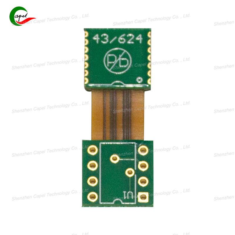
PCBs—whether rigid, flexible (FPC), or rigid-flex—are the "nervous systems" of electronics. But even small flaws in design or manufacturing can lead to failures: a smartphone that shuts down unexpectedly, a medical sensor that gives wrong readings, or a drone that crashes mid-flight. Below are the most common PCB failure modes, plus expert-backed prevention methods tailored to FPC and rigid-flex designs.
Before fixing failures, it’s critical to understand their roots. These four issues plague most PCBs—especially flexible and hybrid designs.
What it looks like: Thin copper traces (the "wires" on PCBs) crack, split, or peel away from the substrate. In FPCs, this often happens at flex zones; in rigid-flex PCBs, it’s common near the rigid-flex transition.
Real-world impact: A fitness tracker’s FPC with a cracked trace might stop recording heart rate mid-workout. A rigid-flex PCB in a car’s infotainment system could cause the touchscreen to freeze.
Why it happens:
- FPCs: Repeated bending beyond the minimum radius (e.g., a 0.1mm thick FPC bent at 0.3mm radius).
- Rigid-flex: Abrupt transitions (no buffer zone between rigid and flex sections) that concentrate stress on traces.
What it looks like: Solder joints (which attach components to PCBs) become brittle, crack, or separate from pads. In FPCs, this often affects connectors; in rigid-flex, it’s common on components near flex zones.
Real-world impact: A wireless earbud’s FPC with a failed solder joint might cut out during calls. A rigid-flex PCB in a satellite could lose communication with Earth if a sensor’s solder joint breaks.
Why it happens:
- FPCs: Using rigid solder paste on flexible sections (it can’t bend with the FPC).
- Rigid-flex: Components placed too close to flex zones (vibrations or bending pull on joints).
What it looks like: Layers (substrate, copper, cover film) peel apart, forming bubbles or gaps. In FPCs, this often starts at the edges; in rigid-flex, it’s common at the rigid-flex bond line.
Real-world impact: A foldable phone’s FPC with delaminated layers might develop a "dead spot" on the screen. A rigid-flex PCB in a industrial sensor could short-circuit if moisture seeps into gaps.
Why it happens:
- FPCs: Low-quality adhesive (can’t withstand repeated bending) or trapped air during lamination.
- Rigid-flex: Mismatched thermal expansion (rigid FR-4 and flexible PI expand at different rates when heated).
What it looks like: Copper traces turn green or black (oxidation) and lose conductivity. In FPCs, this affects exposed pads; in rigid-flex, it’s common in harsh environments (e.g., near water or chemicals).
Real-world impact: A smartwatch’s FPC with corroded traces might drain battery quickly. A rigid-flex PCB in a marine device could fail if saltwater corrodes its power traces.
Why it happens:
- FPCs: Missing or damaged cover film (exposes copper to sweat or dust).
- Rigid-flex: No conformal coating (protective layer) for sections in humid/chemical environments.
The good news? Most failures are avoidable with targeted design choices. Below are tips for FPCs and rigid-flex PCBs, tested by PCB engineers.
Follow Minimum Bend Radius Rules
- Use the "5x thickness" guideline: A 0.1mm thick FPC needs a minimum 0.5mm bend radius. For critical applications (e.g., medical devices), increase it to 8x thickness.
- Test with a bend simulator: Run 10,000+ bend cycles (mimicking real use) and check for trace cracks.
Use Flexible Solder Paste and Reinforce Critical Areas
- Choose "flexible solder paste" (contains rubber particles) for components on flex zones—it bends without cracking.
- Add reinforcement patches (e.g., PI film) to connector areas: This distributes stress and prevents solder joint failure.
Optimize Lamination and Cover Film
- Use high-quality adhesive (peel strength ≥1.5N/cm) to bond layers—avoid cheap adhesives that peel.
- Ensure full air removal during lamination: Use vacuum presses to eliminate bubbles that cause delamination.
Seal Exposed Areas
- Cover all exposed copper pads with solder mask or conformal coating (silicone works for FPCs).
- For wearables, use moisture-resistant cover film (e.g., PTFE-based) to block sweat.
Design Gradual Transitions and Buffer Zones
- Add a 3–5mm buffer zone between rigid and flex sections: No components or traces here—this spreads stress.
- Use "teardrop" trace shapes near transitions: Wide at the rigid end, narrow at the flex end—prevents trace cracking.
Match Materials for Thermal Expansion
- Choose rigid and flex materials with similar Tg (glass transition temperature): e.g., high-Tg FR-4 (Tg=170°C) for rigid sections and PI (Tg=280°C) for flex—minimizes delamination when heated.
- Use "transition adhesives" (designed for mixed materials) to bond rigid and flex layers.
Place Components Strategically
- Keep heavy components (e.g., chips, connectors) on rigid sections only—never on flex zones.
- For components near flex zones, use "floating" footprints: Leave small gaps (0.1mm) between pads and traces to absorb bending stress.
Add Environmental Protection
Founded in 2009, our company has deep roots in the production of various circuit boards. We are dedicated to laying a solid electronic foundation and providing key support for the development of diverse industries.
Whether you are engaged in electronic manufacturing, smart device R&D, or any other field with circuit board needs, feel free to reach out to us via email at sales06@kbefpc.com. We look forward to addressing your inquiries, customizing solutions, and sincerely invite partners from all sectors to consult and collaborate, exploring new possibilities in the industry together.
