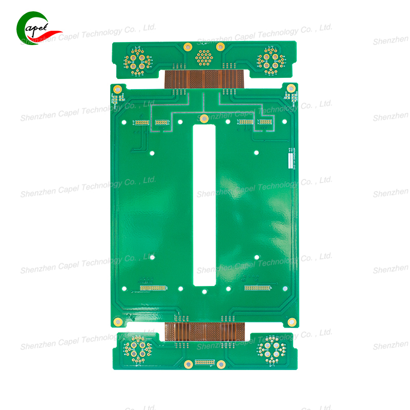
Flexible Printed Circuits (FPCs) are the hidden backbone of bendable gadgets—from foldable phones to wearable sensors. But turning a thin polyimide film into a functional FPC takes precision, strict processes, and careful quality checks. Whether you’re a seasoned engineer or new to FPC production, this guide breaks down the core steps and tips to avoid common pitfalls.
FPC production is a step-by-step dance of material preparation, etching, and assembly. Here’s how it works:
1. Substrate Preparation: The Foundation
The process starts with the base material—usually a thin polyimide (PI) film (12.5–50μm thick). First, the PI film is cleaned to remove dust, oils, or residues (even tiny contaminants can ruin later steps). Then, a layer of adhesive is applied to bond the film to copper foil (the material for conductive traces). This “PI + adhesive + copper” sandwich is pressed firmly to ensure no bubbles form—bubbles would create weak spots that break during bending.
2. Circuit Patterning: Etching the “Roads”
Next, engineers transfer the circuit design (from a digital file) onto the copper layer using a process called “photolithography.” Here’s the breakdown:
-
A light-sensitive “photoresist” is coated onto the copper.
-
The design is projected onto the photoresist—exposed areas harden, while unexposed areas stay soft.
-
The soft photoresist is washed away, leaving a “stencil” of the circuit.
-
The board is dipped in an etching solution (like ferric chloride), which eats away the unprotected copper. What’s left? The thin copper traces that carry electrical signals.
3. Cover Layer Lamination: Adding Protection
To shield the fragile copper traces, a cover layer (usually PI film with adhesive) is laminated onto the board. This step requires precise alignment—if the cover layer is off by even 0.1mm, it might block solder pads (where components connect). The board is then heated and pressed to ensure the cover layer sticks tightly, with no gaps for moisture or dust to seep in.

4. Drilling & Plating: Connecting Layers (for Multi-Layer FPCs)Multi-layer FPCs need holes (called “vias”) to connect copper traces across layers. Tiny holes (as small as 0.1mm) are drilled using lasers or mechanical drills—lasers are better for thin films, as they avoid cracking the PI. Then, the holes are plated with copper to make them conductive, ensuring signals flow smoothly between layers.
5. Component Assembly: Bringing It to Life
Finally, electronic components (like chips or connectors) are soldered onto the FPC’s solder pads. For tiny FPCs (e.g., in smartwatches), this uses “surface-mount technology (SMT)” —a machine places components with precision, and the board is heated to melt the solder. After soldering, the FPC is tested to ensure all connections work.
Even small mistakes in FPC production can lead to broken circuits or failed devices. Here are the most critical quality checks:
1. Inspect for Copper Trace Damage Early
After etching, use a high-magnification camera (or automated optical inspection, AOI) to check for thin, broken, or shorted traces. A trace that’s too thin (less than 0.05mm) will break when bent; a shorted trace (two traces touching) will cause a device to short-circuit. Catching these issues now saves time and cost later.
2. Test Adhesion Strength
Weak adhesion between layers (PI, copper, cover layer) is a top cause of FPC failure. Use a “peel test”: gently pull the cover layer or copper foil—if it peels off easily (less than 1.5N/cm of force), the adhesive is faulty. This test ensures the FPC can handle repeated bending without layers separating.
3. Check Cover Layer Alignment & Pinholes
Use a coordinate measuring machine (CMM) to verify the cover layer is aligned correctly—misalignment blocks solder pads. Also, check for pinholes (tiny holes in the cover layer) with a light test: hold the FPC up to a light—if light shines through, pinholes are present, which let moisture damage copper traces.
4. Validate Flexibility with Bend Testing
Simulate real-world use with a bend tester: fold the FPC back and forth (e.g., 10,000 times at a 180° angle) and test conductivity after each 1,000 cycles. If the signal drops or stops, the FPC fails—this ensures it can survive the wear and tear of devices like foldable phones.
Founded in 2009, our company has deep roots in the production of various circuit boards. We are dedicated to laying a solid electronic foundation and providing key support for the development of diverse industries.
Whether you are engaged in electronic manufacturing, smart device R&D, or any other field with circuit board needs, feel free to reach out to us via email at sales06@kbefpc.com. We look forward to addressing your inquiries, customizing solutions, and sincerely invite partners from all sectors to consult and collaborate, exploring new possibilities in the industry together.