Why High-Density PCBs Are Critical for Next-Gen Consumer Electronics
Date: 2025-08-16
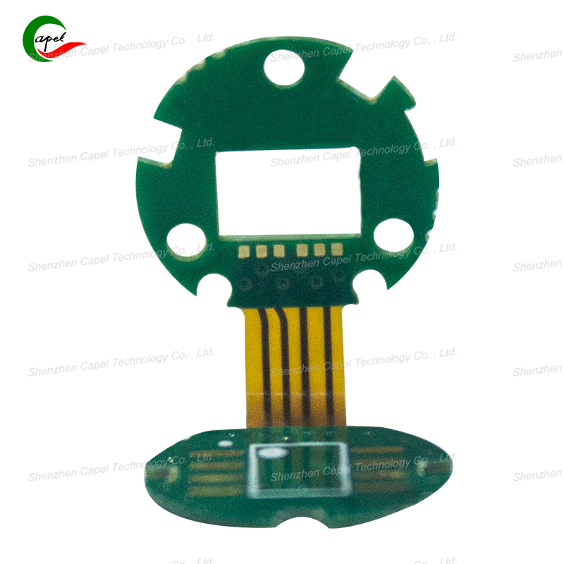
The next generation of consumer electronics—think foldable phones with 8K screens, tiny smartwatches that monitor blood sugar, or wireless earbuds with 24-hour battery life—isn’t just about “new features.” It’s about packing more power, more sensors, and more functionality into devices that keep getting smaller. And the unsung hero making this possible? High-Density PCBs (HDPCBs). Unlike standard PCBs with wide traces and large component gaps, HDPCBs cram more circuits, smaller parts, and tighter connections into the same (or smaller) space. Let’s break down why they’re non-negotiable for the gadgets of tomorrow.
Today’s consumers want devices that fit in their pockets but perform like laptops. A standard PCB can’t keep up—its wide copper traces and large solder pads take up too much space. HDPCBs solve this with:
-
Tiny traces & pads: HDPCBs use traces as narrow as 0.075mm (thinner than a human hair) and solder pads as small as 0.2mm. This lets engineers fit 2–3x more circuits on the same board size.
-
Microvias: These are tiny holes (as small as 0.1mm) that connect layers of the PCB without wasting space. For example, a next-gen smartwatch needs to fit a heart rate sensor, GPS chip, and battery in a 40mm case—HDPCBs with microvias let all these components communicate without bulky wiring.
Without HDPCBs, that smartwatch would either be bulkier or lose key features.
Next-gen devices rely on 5G and AI—technologies that demand ultra-fast signal speeds and minimal delay. Standard PCBs cause “signal loss” (signals weaken as they travel) and “cross-talk” (signals interfere with each other), which slows down 5G and AI processing. HDPCBs fix this by:
-
Controlled impedance: HDPCBs are designed to keep signal resistance (impedance) consistent across the board, so 5G signals don’t fade mid-transmission.
-
Tighter spacing with isolation: Even though traces are close together, HDPCBs use special materials (like low-loss substrates) to block cross-talk. This is critical for AI-powered devices like smart cameras—they need to process 4K video in real time, and any signal interference would ruin image quality.
Tomorrow’s gadgets won’t just “work”—they’ll “sense” and “adapt.” A foldable phone might have 10+ sensors (for fold detection, pressure, and temperature); a smart ring could track heart rate, sleep, and blood oxygen. Each sensor needs a connection to the device’s brain (the processor), and HDPCBs make this possible by:
-
High component density: HDPCBs can hold hundreds of tiny surface-mount components (SMDs) per square inch—far more than standard PCBs. For example, a wireless earbud with a HDPCB can fit a noise-canceling chip, a battery management system, and a motion sensor in a case smaller than a thumbnail.
-
Multi-layer design: HDPCBs often have 8–12 layers (vs. 2–4 for standard PCBs), with each layer dedicated to a different function (power, signals, sensors). This keeps the board thin but super functional—perfect for devices like smart glasses, where every millimeter of space counts.
No one wants a gadget that dies after 2 hours. HDPCBs help extend battery life by:
Founded in 2009, our company has deep roots in the production of various circuit boards. We are dedicated to laying a solid electronic foundation and providing key support for the development of diverse industries.
Whether you are engaged in electronic manufacturing, smart device R&D, or any other field with circuit board needs, feel free to reach out to us via email at sales06@kbefpc.com. We look forward to addressing your inquiries, customizing solutions, and sincerely invite partners from all sectors to consult and collaborate, exploring new possibilities in the industry together.
