
Date: 2026-07-22
You're a hardware engineer or a product manager developing a new product. You spend weeks perfecting the schematic, carefully completing the layout and routing. With confidence, you send your design files to a factory. A week later, the reply comes: “This design can't be manufactured. Trace widths are too thin. Clearance is insufficient. The aspect ratio exceeds our capability. You need to redesign.”
This is one of the most common and frustrating scenarios in hardware development. The design works — but it can't be manufactured. The problem isn't your circuit function. It's that you didn't consider how the factory would make it during the design phase.
That's the cost of disconnection between PCB design and manufacturing. In this guide, I'll walk you through the complete PCB design process, manufacturing requirements, and how to bridge the gap between the two. Plain English, no fluff.
PCB design never starts with opening software and drawing lines. It starts with the schematic and component selection.
The schematic is the functional blueprint — it defines which components connect to which, how signals flow, and how power is distributed. Get the schematic right, and the rest follows. Get it wrong, and everything else is wasted effort.
Component selection is often underestimated. Are your chosen components in stock? Are they standard packages? Does the pin pitch match your manufacturing capabilities? If you don't think about these questions during selection, they become problems during manufacturing.
Good design considers manufacturability from component selection — choosing common, available, standard-package components is always smarter than choosing a “better-performing but unavailable” part.
After the schematic, the next step is PCB placement and routing.
Placement determines the board's success. Where components go directly affects signal integrity, manufacturability, and EMI performance. Good placement follows core principles:
Place critical components first — connectors, MCUs, power ICs
Modular zoning — separate analog, digital, and power sections
Leave sufficient clearance — between components and between components and board edges
Routing turns “logical connections” into “physical connections”. Routing isn't just about “connecting the dots” — trace width, length, spacing, and reference planes all directly affect signal quality and manufacturability.
High-speed signals (USB, DDR, MIPI, PCIe) require controlled impedance. Wrong impedance means signal reflection, eye diagram closure, and device failure. Impedance depends on trace width, copper thickness, distance to the reference plane, and dielectric constant — all of which must be calculated during routing, not discovered during manufacturing.
This is the most important section. DFM (Design for Manufacturing) is a set of rules and checks that ensure a PCB can be fabricated and assembled with high yield. In simple terms: think about how the factory will make it while you're designing it, not after.
In 2026, DFM is no longer a “post-design check” — it's a mindset that runs through the entire design process. Core DFM rules include:
Trace Width and Spacing: The factory's etching process determines minimum trace width and spacing. Your design must stay above these minimums. A good rule: always design traces wider than the minimum if space allows.
Hole Size and Aspect Ratio: Board thickness divided by hole diameter is the aspect ratio. If it's too large, copper plating won't reach the middle of the hole wall. Generally, keep the aspect ratio below 8:1.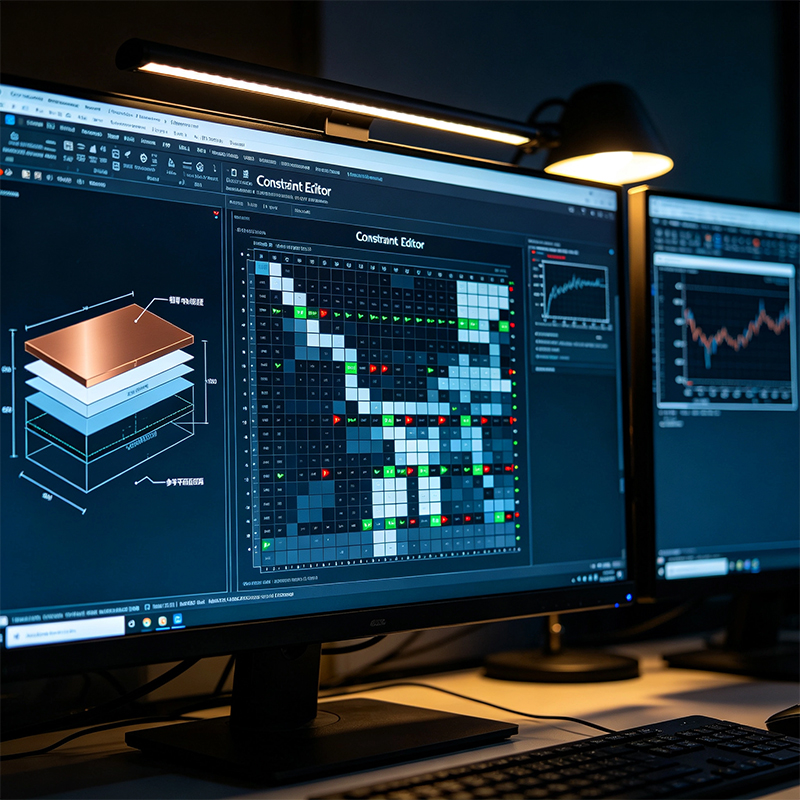
Annular Ring: There must be enough copper ring around each drilled hole. Drill misalignment combined with a thin annular ring means the trace breaks.
Panelization and Tooling Strips: For SMT assembly efficiency, small boards need to be panelized into larger panels. Panelization must be planned during design — tooling strips for the assembly line, V-cut or mouse bites for depaneling.
Solder Mask Dams: Fine-pitch components (below 0.5mm pitch) need sufficient solder mask dam width to prevent bridging.
If your product uses flex PCBs, rigid-flex boards, or HDI boards, the design rules are completely different from rigid boards.
Flex PCB Design:
No components or vias in bend areas — solder joints crack under bending
Bend radius at least 10× board thickness (for dynamic bending)
Traces perpendicular to the bend line, not parallel
Use rolled annealed (RA) copper instead of ED copper — RA copper is more fatigue-resistant
Rigid-Flex Design:
Clearly define flex-to-rigid transitions, specifying bend type and stackup requirements
No vias or pads at the transition — this is the most fragile point
Use curved routing instead of 90° angles in flex zones to optimize stress distribution
Rigid-flex can replace multiple rigid boards, connectors, and wire harnesses by folding into 3D space
HDI Design:
Laser-drilled microvias instead of mechanical through-holes — minimum diameter down to 0.075mm
Route high-speed signals as stripline, not microstrip
HDI “order” determines manufacturing difficulty — 1-order is simplest, any-layer is most complex
2026 HDI trends: ultra-fine traces, AI-assisted layout, thermal management (AI boards can reach 300W/in² power density)
After design completion, you need to convert your design into manufacturing files that factories can read. A complete manufacturing package includes:
Gerber files (all copper layers, solder mask, silkscreen, board outline)
Excellon drill file (hole locations, sizes, plating information)
BOM (all components)
Pick-and-Place file (component locations and orientations)
Fabrication notes (board thickness, layer count, material, impedance requirements, surface finish)
Before submitting, run a DRC (Design Rule Check) — check for opens, shorts, and clearance violations. After submitting, preview every layer with a Gerber viewer to confirm information is correct.
The traditional workflow is: designer finishes → sends to factory → factory says “can't make it” → designer revises → sends again… weeks lost in back-and-forth.
A better approach: align design with manufacturing capability from the start. Know your factory's minimum trace width, layer count capability, flex bend radius rules — design with these constraints in mind, and your board passes on the first submission.
That's why more hardware teams are choosing turnkey PCBA services — one supplier handles PCB fabrication, component sourcing, SMT assembly, and testing. Designers only submit design files; the supplier turns them into production-ready boards.
PCB design isn't “done when it's drawn” — it must be aligned with manufacturing to become a usable product.
From schematic to component selection, from placement and routing to DFM checks, from flex/rigid-flex/HDI special rules to final manufacturing output — every step directly affects whether your board can be made, and how well it performs.
If you're designing a new product, or wondering how to turn your design into a manufacturable physical product, send us your requirements. We'll step in during the design phase, run DFM checks, and ensure your design is “manufacturable” from day one.
When you contact us, please include:
Design files (Gerber or source)
BOM
Product type and application
We'll give you an honest answer — what we can do, what we can't, and how to modify your design to make it work.

Kaboer manufacturing PCBs since 2009. Professional technology and high-precision Printed Circuit Boards involved in Medical, IOT, UAV, Aviation, Automotive, Aerospace, Industrial Control, Artificial Intelligence, Consumer Electronics etc..


 English



 Wechat
 +86 13670210335
 +86 13670210335
 E-mail