Date: 2025-10-08
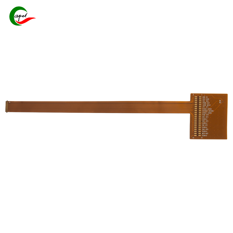
If you’ve ever held a flexible PCB and wondered how thin these things can actually get—you’re not alone. It’s a question I get a lot, especially from startups trying to shrink their designs. But here’s the reality: thinness isn’t just a number. It’s a trade-off.
Let’s break down what really determines how thin a flex PCB can be.
The Two-Layer Reality: It’s All About Base and Copper
At its simplest, a flex PCB is basically two things: a base layer (we usually use polyimide) and a copper circuit layer. The base is thin—anywhere from 0.025 mm to 0.1 mm, honestly thinner than a strand of hair. The copper? Even thinner: think 0.005 mm to 0.01 mm, like one-tenth of that hair.
Stack them together, and you’re looking at a total thickness starting around 0.03 mm. At that level, you don’t just handle it—you baby it.
What’s Actually Used in the Real World
In production, thickness tends to fall into three buckets:
The Go-To: 0.05 mm – 0.1 mm
This is the industry sweet spot. Think AirPods Pro internals—around 0.07 mm thick. It’s thin enough to tuck into tight spots but still survives automated assembly and real-world use. We’ve tested a lot of options, and this range just… works.
The Niche Pick: 0.03 mm – 0.05 mm
You see this in medical wearables or smart rings. A skin-side heart sensor, for instance, might use 0.04 mm. Any thicker, and the user feels it. Any thinner, and yields drop. We learned that balance the hard way.
The Lab Special: ~0.02 mm
Yes, it’s possible. No, you don’t want to mass-produce it. These boards are unbelievably delicate—think “handle-with-tweezers” delicate. I’ve seen them crack just from being looked at wrong.

The Three Big Reasons We Can’t Go Thinner (Yet)
Pushing below 0.03 mm sounds cool in a meeting—until you run into these real-world barriers:
They’re Fragile—Like, Really Fragile
A 0.03 mm board can crease if you pick it up wrong. Try bending it a few thousand times? Microcracks. We once tested a 0.025 mm version: 30% failure rate before it even left the lab.
They Can’t Hold Components Well
Soldering parts onto something this thin is like trying to grill on Saran Wrap. The board warps, the copper lifts… it’s a mess. Even a tiny chip can cause sag or misalignment.
Costs Spike and Yields Tumble
Thin boards are harder to make. Way harder. Imagine trying to spread peanut butter on tissue paper—that’s what lamination feels like. Yields can drop to 70%, and trust me, Finance will have questions.
So… What Should You Choose?
Here’s my rule of thumb:
Use 0.05–0.1 mm for most consumer gear—smartwatches, earbuds, anything that needs to be tough and affordable.
Use 0.03–0.05 mm only when you have no other choice—think medical patches or jewelry-style wearables where every micron matters.
Bottom line: going thinner isn’t about being cutting-edge—it’s about whether you can live with the compromises. In my experience, thicker often means cheaper, faster, and more reliable. And in product design, reliability still wins every time.
related link:
Kaboer manufacturing PCBs since 2009. Professional technology and high-precision Printed Circuit Boards involved in Medical, IOT, UAV, Aviation, Automotive, Aerospace, Industrial Control, Artificial Intelligence, Consumer Electronics etc..