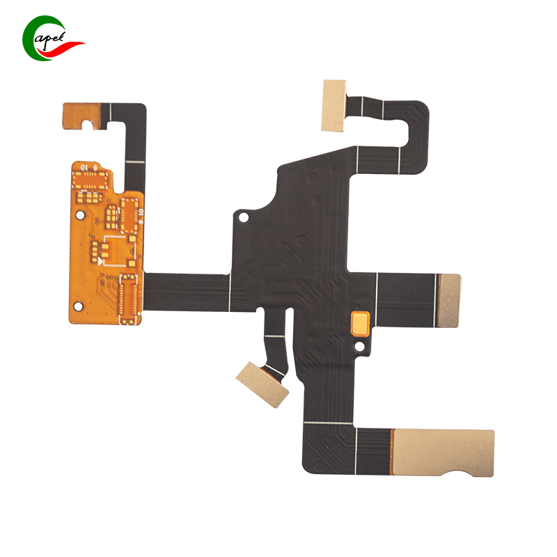
Impedance matching is the unsung hero of high-frequency flexible PCB performance. Get it wrong, and signals degrade, leading to dropped connections, slow data transfer, or even complete failure—especially in 5G devices, IoT sensors, or radar systems. Unlike rigid PCBs, flexible designs add unique twists to impedance calculations. Here’s what engineers need to watch for.
The substrate (the flexible base material) is the foundation of impedance, and its traits are far less stable than rigid FR-4.
- Dielectric Constant (Dk) Variability: Polyimide (PI), the most common flexible substrate, has a Dk around 3.0–3.5—but it shifts with temperature, humidity, and even bending. A PCB bent repeatedly may see Dk fluctuate by ±0.3, throwing off impedance by 5–10%. Always use the manufacturer’s dynamic Dk specs (tested under flexing) instead of static values.
- Thickness Inconsistencies: Flexible substrates are thinner (0.025mm–0.1mm) than rigid ones, and slight thickness variations (as little as 0.005mm) drastically change impedance. For example, a 10% reduction in substrate thickness can increase impedance by 8–12%. Specify tight tolerance (±0.002mm) for high-frequency designs.
Trace dimensions directly impact impedance, but flexible PCBs demand extra precision due to their thin, bendable nature.
- Width vs. Thickness Balance: A trace’s width (W) and copper thickness (T) must be calibrated. For a 50Ω microstrip (a common impedance target), a wider trace lowers impedance, while thicker copper raises it. But in flexible PCBs, thin copper (12μm–35μm) is standard—so even a 5μm increase in thickness (from 18μm to 23μm) can push impedance from 50Ω to 55Ω. Use field solver software to model this interplay.
- Edge Roughness: Rolled copper (used for flexibility) has a rougher surface than electrodeposited copper. This roughness increases signal loss at high frequencies (above 1GHz) and skews impedance calculations. Add a "roughness factor" (typically 0.5–1.0μm) to your field solver inputs to compensate.
A solid ground plane is non-negotiable for impedance control, but flexible PCBs make it trickier to maintain.
- Ground Plane Continuity: Flexing can cause micro-cracks in ground planes, especially if they’re routed through bend zones. A broken ground plane creates impedance spikes. Design ground planes with rounded corners in bend areas and avoid slits or cutouts—even small gaps disrupt the return path, increasing impedance variability.
- Distance from Trace to Ground: The spacing (H) between the signal trace and ground plane is a key impedance driver (closer = lower impedance). In flexible PCBs, this distance can shift when bent—compressing H on the inner curve and stretching it on the outer curve. For dynamic applications (e.g., foldable phones), simulate impedance at the minimum bend radius to ensure it stays within tolerance (±5Ω for most high-frequency uses).
Flexible PCBs often use protective cover layers (PI or PET) and adhesives, both of which affect impedance.
- Cover Layer Dielectric: A 0.01mm PI cover layer has a Dk of ~3.2, similar to the substrate, but it adds to the total dielectric thickness. Ignoring it can lead to a 10–15% impedance error. Include cover layer thickness and Dk in your calculations—field solvers like Polar SI9000 let you model multi-layer dielectrics.
- Adhesive Impact: Epoxy adhesives (used to bond layers) have a higher Dk (4.0–4.5) than PI. If adhesive seeps between the trace and ground plane (common in low-quality manufacturing), it lowers H effectively, reducing impedance. Specify adhesive-free designs for critical high-frequency paths to avoid this variability.
Unlike rigid PCBs, flexible ones face mechanical and environmental stress that warps impedance over time.
- Thermal Effects: PI’s Dk drops by ~0.1 for every 10°C increase, which can raise impedance by 2–3Ω in a 50°C temperature swing (common in automotive or industrial settings). For outdoor sensors, simulate impedance at -40°C to 85°C to ensure it stays within specs.
- Cyclic Flexing: Repeated bending (e.g., 10,000+ cycles in a foldable device) thins the substrate near bend zones, increasing H and raising impedance. Test prototypes under flex cycles and measure impedance post-test—if it drifts more than 10%, adjust trace width or substrate thickness to compensate.
Even the best designs fail if they ignore factory limits.
- Etching Variability: Flexible PCB manufacturers typically hold trace width tolerances of ±0.01mm, but this can widen to ±0.02mm for very thin traces (<0.1mm). A 0.02mm width increase can lower 50Ω impedance to 45Ω. Design with a "buffer"—target 52Ω in simulations to account for etching shifts, ensuring the final product lands at 50Ω ±5%.
- Plating Thickness: Gold or tin plating adds 1–3μm to copper traces, slightly increasing thickness (T) and raising impedance. Include plating in your trace thickness calculations—even a 2μm layer can add 3–5Ω to a 50Ω design.
Simulations are critical, but nothing beats real-world testing. Fabricate a small batch of prototypes and measure impedance with a time-domain reflectometer (TDR) at rest, under flex, and across temperatures. Compare results to simulations—any gaps (e.g., a 7Ω drift under bending) point to missing variables in your model (like unaccounted cover layer shifts).
In flexible PCB design, impedance isn’t a one-and-done calculation—it’s a balance of material science, geometry, and real-world stress. By sweating these details, engineers ensure signals stay strong, even as the PCB bends, heats up, or endures the rigors of daily use.
Founded in 2009, our company has deep roots in the production of various circuit boards. We are dedicated to laying a solid electronic foundation and providing key support for the development of diverse industries.
Whether you are engaged in electronic manufacturing, smart device R&D, or any other field with circuit board needs, feel free to reach out to us via email at sales06@kbefpc.com. We look forward to addressing your inquiries, customizing solutions, and sincerely invite partners from all sectors to consult and collaborate, exploring new possibilities in the industry together.
