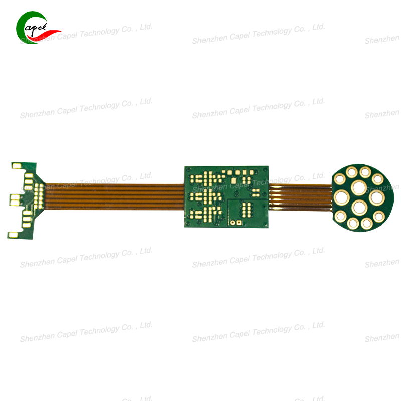
Rigid-flex PCBs blend the stability of rigid boards and the flexibility of FPCs—making them ideal for tight, moving spaces in devices like medical implants or foldable phones. But their hybrid design also creates unique challenges: a small mistake in flex-rigid transition or trace layout can turn a promising project into a costly failure. Below are the most common pitfalls engineers face, plus how to avoid them with proven best practices.
Why it’s a problem: The flexible section (flex zone) of a rigid-flex PCB isn’t indestructible. Many designers treat it like a “bend-any-way” material, only to find it cracks after 100 uses instead of 10,000. For example, a smartwatch PCB with a flex zone bent at a 5mm radius (too tight) might fail after a month of wrist movements—users will complain about unresponsive screens.
Best practice:
- Follow “minimum bend radius” rules: For most polyimide-based flex zones, the minimum bend radius should be 5x the flex zone thickness (e.g., a 0.2mm thick flex zone needs a 1mm radius).
- Test with a bend simulator early: Simulate real-world use (e.g., 10,000 bends at 90°) to check if traces crack or layers peel.
Why it’s a problem: The area where rigid and flex sections meet (the “transition zone”) is a stress hotspot. If the transition is too abrupt—e.g., rigid components ending 1mm from the flex zone—stress concentrates here, causing the PCB to split. A drone’s rigid-flex PCB with a bad transition might break mid-flight when the propeller arms move.
Best practice:
- Add a “buffer zone”: Keep rigid components (like chips or capacitors) at least 3mm away from the flex zone.
- Use “teardrop” pads: Shape solder pads near the transition like teardrops (wide at the rigid end, narrow at the flex end) to spread stress evenly.
Why it’s a problem: Flex zones need to bend freely, but some designers attach heavy components (like connectors or resistors) directly to them. This adds weight and rigidity, making the flex zone prone to breaking. A wireless earbud’s rigid-flex PCB with a connector on the flex zone might stop working after a few weeks—every time the user inserts the charging cable, stress pulls the flex zone apart.
Best practice:
- Keep flex zones “component-free”: Place all heavy or rigid components on the rigid sections.
- Use “flex-to-rigid” connectors: If components must be near the flex zone, use small, lightweight connectors that won’t restrict bending.
Why it’s a problem: High-frequency devices (like 5G phones or radar sensors) rely on consistent impedance (signal resistance) to avoid signal loss. Many designers focus on impedance in rigid zones but ignore flex zones—when the flex zone bends, trace spacing changes, disrupting impedance. This leads to dropped calls in 5G phones or blurry images in smart cameras.
Best practice:
- Design flex zone traces for “bend-friendly impedance”: Use wider traces or adjust dielectric thickness (the material between traces) to keep impedance stable when bent.
- Test impedance under bending: Use a network analyzer to check impedance while the flex zone is bent to its maximum radius—ensure it stays within the target range (e.g., 50Ω ±10%).
Why it’s a problem: To cut costs, some designers use low-grade polyimide or adhesive for flex zones. These materials crack easily or peel apart under repeated bending. A medical device’s rigid-flex PCB with cheap flex material might fail inside a patient’s body—putting lives at risk.
Best practice:
Founded in 2009, our company has deep roots in the production of various circuit boards. We are dedicated to laying a solid electronic foundation and providing key support for the development of diverse industries.
Whether you are engaged in electronic manufacturing, smart device R&D, or any other field with circuit board needs, feel free to reach out to us via email at sales06@kbefpc.com. We look forward to addressing your inquiries, customizing solutions, and sincerely invite partners from all sectors to consult and collaborate, exploring new possibilities in the industry together.
