Date: 2025-12-24
SMD PCB Assembly, short for Surface Mount Device Printed Circuit Board Assembly, is the predominant method for populating modern circuit boards. It involves mounting miniature electronic components directly onto the surface of a PCB using automated machinery, as opposed to inserting leads through holes. This guide explains the SMD assembly process, its critical advantages, and key considerations for selecting a manufacturing partner.
SMD Assembly is a subset of the broader PCB Assembly (PCBA) process, specifically focusing on Surface Mount Technology (SMT). Components used in this process are called Surface Mount Devices (SMDs)—small, leadless parts with metallic termination pads designed for soldering directly onto PCB pads.
The Core Distinction: SMT vs. Through-Hole
Through-Hole Assembly: Components with wire leads are inserted into drilled holes.
SMD (SMT) Assembly: Components are placed and soldered directly onto the board's surface. This enables miniaturization, higher component density, and full automation.

A professional SMD assembly line consists of a series of automated and controlled stages:
Step 1: Solder Paste Printing
A stainless steel stencil is aligned over the PCB. Solder paste (a mix of fine solder particles and flux) is pushed across it by a squeegee, depositing precise amounts onto the component pads. Quality Check: Solder Paste Inspection (SPI) machines use lasers to verify paste volume and alignment.
Step 2: Automated Component Placement
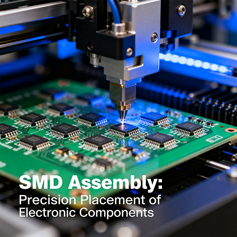
A high-speed pick-and-place machine picks SMD components from reels, sticks, or trays using vacuum nozzles. It then places them with extreme accuracy (often within microns) onto the solder-paste-coated pads. This is the heart of the SMD assembly line.
Step 3: Reflow Soldering
The populated PCB travels through a reflow oven on a conveyor. It passes through carefully controlled heating zones that melt the solder paste, forming permanent metallurgical solder joints as it cools. The temperature profile is critical for reliability.
Step 4: Inspection & Testing
Automated Optical Inspection (AOI): Cameras scan the board to detect defects like missing/misaligned components, bridging, or insufficient solder.
In-Circuit Testing (ICT) or Flying Probe: Electrical tests verify connections and basic component functionality.
X-Ray Inspection: Used for complex assemblies like Ball Grid Arrays (BGAs) to inspect solder joints underneath the component.
| Benefit | Explanation | Impact on Your Product |
|---|---|---|
| Miniaturization | SMD components are significantly smaller than through-hole equivalents. | Enables smaller, lighter, and more portable end products. |
| Higher Component Density | Components can be placed on both sides of the board with finer pitch. | Allows for more complex functionality in a compact space. |
| Superior Performance | Shorter lead lengths reduce parasitic inductance/capacitance. | Improves signal integrity and high-frequency performance. |
| Automation & Speed | The process is highly automated from printing to placement. | Enables high-volume production, consistent quality, and lower labor costs. |
| Cost-Effectiveness | Reduced board drilling, simpler PCB design, and less material usage. | Lower overall assembly cost, especially at scale. |
Selecting the right manufacturer is critical for product success. Key capabilities to evaluate include:
Equipment & Technology: Look for modern high-speed placement machines, multiple SPI/AOI stations, and X-ray capability for BGA assembly.
Process Control & Certifications: A partner with a robust Quality Management System (e.g., ISO 9001) ensures repeatability.
Supply Chain Management: Strong component sourcing and inventory management prevent production delays.
Engineering Support (DFM): The ability to provide Design for Manufacturability feedback before production saves time and cost.
Scalability: Can they seamlessly handle your needs from prototyping to mass production?
At Kaboer, we specialize in delivering high-quality, reliable SMD PCB assembly services tailored to the needs of global electronics brands and innovators. Our own dedicated PCBA factory in Shenzhen, China, places us at the heart of the world's electronics manufacturing ecosystem.
What This Means for You:
Direct Control & Communication: Working with our own factory eliminates middlemen, ensuring faster response times, transparent communication, and direct oversight of your project.
Assured Quality: We maintain complete control over the entire SMD assembly line—from solder paste storage to final inspection—implementing strict quality checkpoints at every stage.
Supply Chain Advantage: Located in Shenzhen, we have immediate access to one of the world's most extensive electronics component markets, ensuring efficient sourcing and cost management.
Scalable Solutions: Whether you need 50 prototypes for R&D or 50,000 units for a product launch, our factory is equipped and managed to scale with your requirements.
Engineering Partnership: Our technical team provides expert DFM analysis to optimize your designs for manufacturability, yield, and reliability before production begins.
Let Kaboer be your trusted extension in Asia. Contact us today to discuss how we can bring your SMD PCB designs to life with precision, efficiency, and clarity.
Q1: Can SMD and through-hole components be used on the same board?
A: Yes. This is called a mixed-technology assembly. The SMD components are placed and reflow-soldered first, followed by through-hole component insertion and wave or selective hand soldering.
Q2: What is the smallest component size you can assemble?
A: Standard assembly handles components down to 0201 metric (008004 inch) size. Advanced lines can place 01005 or even smaller micro-components. This depends on the manufacturer's equipment capabilities.
Q3: How do you ensure reliability for fine-pitch or BGA components?
A: Reliability is ensured through precise process control: accurate solder paste printing via laser-cut stencils, controlled reflow profiles, and post-assembly inspection using AOI and X-ray machines to verify hidden solder joints.
Q4: What files are required to get an SMD assembly quote?
A: You typically need:
Gerber Files (for PCB fabrication)
Bill of Materials (BOM) with manufacturer part numbers
Pick-and-Place File (XYRS coordinates)
Assembly Drawings (for special instructions)
Kaboer manufacturing PCBs since 2009. Professional technology and high-precision Printed Circuit Boards involved in Medical, IOT, UAV, Aviation, Automotive, Aerospace, Industrial Control, Artificial Intelligence, Consumer Electronics etc..