Date: 2025-12-24
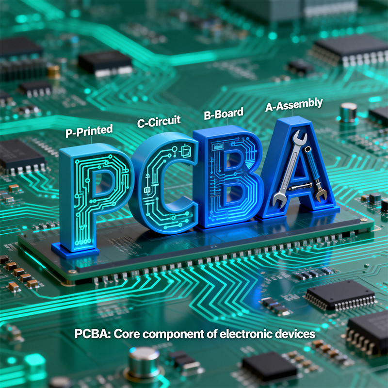
PCBA stands for Printed Circuit Board Assembly. It refers to the complete process of mounting, soldering, and testing electronic components onto a bare printed circuit board (PCB), transforming it from a non-functional substrate into a fully operational electronic assembly. Understanding what PCBA means is crucial for electronics manufacturers to communicate requirements, source services, and manage the transition from design to finished product.
Printed Circuit Board (PCB): The foundational, non-conductive board (substrate) with pre-fabricated copper traces that provide electrical connectivity pathways. A PCB alone has no components.
Assembly (A): The comprehensive manufacturing process of populating the bare PCB with electronic components (resistors, capacitors, ICs, connectors, etc.) and permanently attaching them via soldering to create an electrically functional unit.
In essence: PCB + Components + Assembly Process = PCBA.
A PCBA is also commonly referred to as a "loaded board," "assembled board," or simply an "electronic assembly."
The PCBA process is a sequential series of specialized operations, typically categorized into three main stages:
Stage 1: Solder Paste Application (for SMT)
Process: Solder paste (a mixture of tiny solder balls and flux) is precisely applied to the component pads on the PCB using a stainless steel stencil and a squeegee.
Purpose: This paste will form the electrical and mechanical joint during reflow soldering.
Stage 2: Component Placement
Surface Mount Technology (SMT) Placement: Automated pick-and-place machines use vacuum nozzles to pick SMT components from reels or trays and place them with high speed and precision onto the solder-paste-coated pads.
Through-Hole Technology (THT) Insertion: Leads of larger components (like connectors or transformers) are inserted into drilled holes on the PCB. This can be done manually for prototypes or with automated insertion machines for high-volume production.
Stage 3: Soldering
Reflow Soldering (for SMT): The PCB with placed SMT components passes through a multi-zone reflow oven. The controlled heat profile melts the solder paste, forming permanent solder joints as it cools.
Wave Soldering (for THT): The underside of the PCB (with inserted THT component leads) passes over a molten wave of solder, which wets the exposed metal and creates the connections. Selective soldering is often used for mixed-technology or heat-sensitive boards.
Stage 4: Inspection, Testing, and Final Assembly
Automated Optical Inspection (AOI): Cameras scan the PCBA to detect common defects like missing components, misalignment, or solder bridging.
In-Circuit Testing (ICT): Electrical probes test the PCBA to verify correct component values, presence, and basic functionality.
Functional Testing (FCT): The assembled unit is powered on and tested under simulated operational conditions to ensure it performs as per the final product specifications.
Conformal Coating (if required): A protective polymeric layer is applied to shield the assembly from moisture, dust, chemicals, and thermal stress.
Final Assembly: The tested PCBA may be integrated with other sub-assemblies (housings, displays, wiring) to create the final product.
| Feature | PCB (Printed Circuit Board) | PCBA (Printed Circuit Board Assembly) |
|---|---|---|
| State | Bare, unpopulated board. Inactive. | Fully populated with components. Potentially Active. |
| Composition | Substrate (FR-4, etc.), copper layers, solder mask, silkscreen. | PCB + all electronic components (SMT & THT) + solder joints. |
| Functionality | Provides only the physical structure and electrical pathways. | Performs the intended electronic function (e.g., amplification, processing, power conversion). |
| Manufacturing Focus | Fabrication (etching, lamination, drilling). | Assembly, integration, and testing. |
| Visual Cue | Looks "empty" with just pads and traces. | Looks "busy" with a variety of components attached. |
For global electronics manufacturers, understanding and leveraging professional PCBA services is essential because it:
Converts Design into Reality: It is the physical execution phase that turns an electronic schematic and PCB layout into a working device.
Requires Specialized Expertise: Involves sophisticated machinery (pick-and-place, reflow ovens, AOI), precise process control, and skilled technicians.
Impacts Quality & Reliability: The quality of assembly directly determines the performance, longevity, and field failure rates of the final product.
Offers a Scalable Service Model: Manufacturers can outsource PCBA to specialized contract manufacturers (CMs or EMS providers), allowing them to focus on core competencies like design and marketing while leveraging the CM's scale, expertise, and supply chain.
Q1: Does PCBA include the cost of the components?
A: This depends on the service model. Turnkey PCBA means the assembly provider also procures all components and manages the inventory. Consignment PCMA means the customer provides all components, and the provider charges only for the labor and process of assembly.
Q2: What files does a PCBA manufacturer need from me?
A: Essential files include:
Gerber Files: For PCB fabrication.
Bill of Materials (BOM): A complete list of all components with reference designators, part numbers, and quantities.
Pick-and-Place File: Contains X-Y coordinates, rotation, and layer data for automated component placement.
Assembly Drawings: Illustrations showing component locations and orientations.
Q3: How long does a typical PCBA process take?
A: The timeline varies based on complexity and volume. For standard prototypes, it can be 5-10 business days. For new product introduction (NPI) or mass production, the first articles may take 2-4 weeks, including setup and test fixture development.
Q4: What are the main quality control checkpoints in PCBA?
A: Key checkpoints are: Solder Paste Inspection (SPI) post-application, Pre-Reflow Visual Check, Post-Reflow AOI, and finally, Electrical Testing (ICT/FCT). A reputable manufacturer will have a detailed Quality Management System (QMS) governing each step.
Kaboer manufacturing PCBs since 2009. Professional technology and high-precision Printed Circuit Boards involved in Medical, IOT, UAV, Aviation, Automotive, Aerospace, Industrial Control, Artificial Intelligence, Consumer Electronics etc..