Date: 2026-01-06
If you're new to hardware design or managing a procurement project, and you're searching "components of PCB," you're probably thinking: What exactly makes up a circuit board? And why do some boards cost so much more than others?
Open up your smartphone or router, and that green board you see isn't just "a board." It's a multi-layered functional platform where every part affects performance, cost, and reliability.
Think of a PCB as a layered sandwich. From top to bottom, here's what it's made of:
1. The Substrate – The Board's "Foundation"
The most common material is FR-4, a glass-reinforced epoxy laminate. Imagine it as a tough plastic sheet. Its job is to provide structural support and electrical insulation.
What you should know:
Most consumer electronics use FR-4
High-frequency applications (like 5G) may need more expensive specialty materials
Products needing better heat dissipation might use metal-core or ceramic substrates
2. The Copper Layers – The Board's "Highway Network"
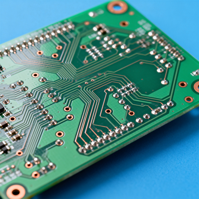
This is the actual circuit. A thin copper foil is chemically etched to create traces on the substrate surface. A simple board might have copper on one side only; complex boards have multiple copper layers, connected vertically by tiny holes (vias).
What you should know:
Copper thickness affects current-carrying capacity (common: 1 oz / 35 µm)
Trace precision impacts signal integrity, especially for high-frequency signals
The copper's surface finish (like ENIG or HASL) affects solderability

3. The Solder Mask – The Board's "Protective Coat"
That green (or other colored) coating is the solder mask. It covers the copper traces where you don't want solder, preventing accidental shorts and protecting the copper from oxidation.
A fun fact: Military PCBs sometimes use black solder mask for lower visibility under infrared. Prototype boards often use blue or red just to distinguish versions.
4. The Silkscreen – The Board's "Road Signs and Addresses"
Those tiny white letters and symbols are the silkscreen. They show where components go ("R1," "C5," "U3") and sometimes include logos or version info.
5. Holes and Vias – The "Elevator Shafts" Connecting Layers
Mounting holes: For screws to attach the PCB to an enclosure
Vias: Tiny tunnels connecting different copper layers
Component holes: For leads of through-hole parts
When you're comparing quotes:
A consumer-grade PCB with FR-4, two copper layers, and standard processes can cost over 10 times less than a communications PCB with high-frequency material, 8+ copper layers, and laser-drilled vias. Knowing these components helps you understand where the money goes.
When your design has issues:
If signals are unstable, check your trace layout and layer stack-up
If soldering is problematic, the copper surface finish might need changing
If performance degrades in humid environments, better substrate and solder mask may be needed
When you need to make choices:
On Kaboer's production lines in Shenzhen, we often help clients balance choices: cheaper FR-4 or more expensive material for better signal integrity? Lower-cost single-sided boards or compact multilayer designs? Each choice is a trade-off.
One of the most interesting things about PCB fabrication is that "what you don't see" matters as much as "what you see." For example, the material and thickness of the insulating layers between copper in a multilayer board are invisible but directly affect signal transmission and heat dissipation. A good manufacturer knows how to optimize these hidden elements.
When working on a PCB-related project, understanding this "language" of components helps you communicate better with manufacturers and make smarter decisions. After all, a PCB isn't just a disposable part—it's the foundational platform for your product's functionality.
Kaboer manufacturing PCBs since 2009. Professional technology and high-precision Printed Circuit Boards involved in Medical, IOT, UAV, Aviation, Automotive, Aerospace, Industrial Control, Artificial Intelligence, Consumer Electronics etc..