Date: 2026-01-06
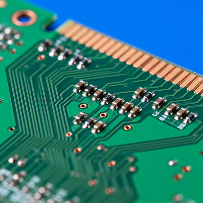
If you've ever opened a smartphone, laptop, or any electronic gadget, you've seen that green (or sometimes other colored) board with fine lines and tiny parts. That board is a PCB—a Printed Circuit Board.
In simple terms, a PCB is the "foundation and road network" of an electronic product. It has two main jobs:
To give electronic components a place to live: providing physical support for chips, resistors, capacitors, and other parts.
To let electricity flow correctly: using etched copper traces, like roads, to guide electrical signals where they need to go.
In manufacturing hubs like Shenzhen, making a PCB is a bit like creating a complex, multi-layered print:
The Design Phase: Engineers first draw the circuit diagram in software, which decides the "traffic plan" for electricity.
The Fabrication Phase:
Material Choice: Most common is FR-4 fiberglass, a tough, paper-like sheet.
"Drawing the Lines": Chemical etching removes unwanted copper, leaving behind the designed circuit traces.
"Drilling Holes": Tiny holes are drilled for mounting components or connecting different layers.
"Adding Color": A solder mask (often green) is applied to protect the copper traces from accidental shorts.
A simple PCB might have just one layer of copper. A complex motherboard can be like a "layer cake," with over a dozen different circuit layers stacked together and connected through microscopic holes.
You might think, "It's just a board, right?" But in a real product, the quality of the PCB directly affects:
Product Reliability: A good PCB should withstand bending, vibration, and temperature changes. Poor-quality PCBs can suffer from broken traces or delamination.
Signal Integrity: High-speed signals (like USB 3.0 or HDMI) demand extreme precision in the PCB traces. Bad trace design is like driving a race car on a potholed road—the signal gets corrupted.
Production Cost: PCB design impacts manufacturing efficiency. For example, poor component placement might require more manual work, increasing cost.
Safety & Certification: PCBs for certain fields (medical, automotive) must meet strict safety standards.
Here's a common point of confusion: a PCB by itself is empty. It's just a board with printed lines. Only after all the electronic components are mounted and soldered onto it does it become a PCBA (Printed Circuit Board Assembly).
This process—electronics manufacturing—is like building houses on developed land. The PCB provides the foundation and roads; mounting and soldering the components builds the functional community.
At the Kaboer factory in Shenzhen, our daily work is helping clients take this step: turning designed PCBs into working PCBAs through precise equipment and processes. We've seen projects where the PCB design was excellent, but poor component choice or manufacturing led to disappointing results. We've also seen seemingly simple PCB designs turned into highly reliable products through optimized manufacturing.
If you're new to this, remember this simple distinction: the PCB is the stage, the PCBA is the full performance. When looking for a manufacturing partner, don't just ask if they can make the PCB. Ask if they can reliably turn that PCB into a PCBA—that's what your product actually needs.
Kaboer manufacturing PCBs since 2009. Professional technology and high-precision Printed Circuit Boards involved in Medical, IOT, UAV, Aviation, Automotive, Aerospace, Industrial Control, Artificial Intelligence, Consumer Electronics etc..