Date: 2026-02-03
As chips in electronic devices become more powerful and compact, a critical challenge emerges: heat. If this heat isn't dissipated promptly, it can lead to chip overheating, throttled performance, or even failure. Beyond familiar heatsinks and fans, a clever and vital design works silently within the circuit board itself—the thermal via.
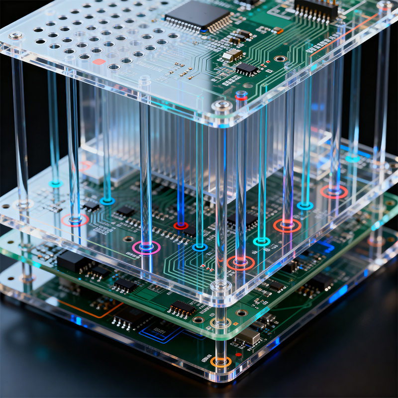
In simple terms, thermal vias are arrays of small, plated holes drilled into a printed circuit board specifically for conducting heat. Unlike regular vias that primarily carry electrical signals, their core mission is to act as "highways for heat", rapidly transferring thermal energy from hot components (like CPUs or power ICs) on the board's surface to inner ground planes or cooling areas on the backside.
Imagine the circuit board substrate as a thermal blanket; standard epoxy or fiberglass materials conduct heat poorly, trapping it under the chip. Thermal vias are like vertical "copper pillars" drilled through this blanket. Copper's thermal conductivity is hundreds of times greater than the insulating board material.
A typical heat flow path is: Heat from the component pad → connected array of thermal vias → copper cylinder within the vias → large ground copper plane inside the board (acting as a superb heat spreader) → further conduction to the board's backside → finally removed by a heatsink, enclosure, or air.
In this process, the inner ground plane acts as a "heat reservoir," quickly spreading the concentrated heat from a point source to prevent local hot spots.
Designing thermal vias isn't as simple as drilling a few holes. Several core factors must be considered:
1. Quantity and Array Density
A single via has limited thermal capacity. Engineers typically design a dense array or grid of thermal vias under or around the footprint of a hot chip. More vias packed closer together create a wider "thermal roadway," significantly boosting heat transfer. Sometimes, a "full grid" covering the entire thermal pad area is used.
2. Hole Size and Copper Thickness
Hole Diameter: Smaller diameters (e.g., 0.3mm) allow more vias in a limited space, increasing the total cross-sectional area for heat conduction. Larger diameters aid manufacturability and filling.
Copper Thickness: The thickness of the copper plating on the hole wall is crucial. Thicker copper plating means lower thermal resistance. Processes like via filling or plugging (filling the hole with conductive epoxy or copper) offer the best possible thermal performance.
3. Connection and Thermal Relief
Thermal Pad Connection: Thermal vias often connect directly to the component's thermal pad on the PCB. To facilitate soldering, vias on pads are sometimes connected with a thermal relief pattern—spokes instead of a solid connection—which prevents excessive heat sinkage during soldering that could cause defects, while still providing a thermal path.
Solder Mask Impact: Note that solder mask is thermally insulating. Ensure that areas where heat needs to exit (like the corresponding spot on the board's back) have the solder mask opened, exposing the copper to directly contact a heatsink or the air.
4. Materials and Stack-up
High-performance board materials (like high-thermal-conductivity FR-4 or metal-core boards) conduct heat better themselves, working synergistically with thermal vias. In multilayer boards, thermal vias can connect to multiple internal ground planes, creating a three-dimensional heat dissipation network.
High-Power Components: LED drivers, motor controllers, power modules.
High-Density Packaged ICs: BGA, QFN packages, especially those with an exposed thermal pad on the bottom.
Space-Constrained Devices: Smartphones, tablets, wearables that cannot accommodate large heatsinks and rely on the PCB itself for cooling.
RF and High-Speed Circuits: These circuits are temperature-sensitive, and stable temperatures help ensure signal integrity.
In summary, thermal vias are a fundamental, effective, and relatively low-cost engineering solution in the thermal management of modern high-density, high-performance electronics. They cleverly integrate the PCB's internal structure into the cooling system. A skilled engineer considers not only the path of electrical signals but also the path of heat flow. As power densities continue to rise, the proper use of thermal vias is often a critical step in ensuring a product's stability, reliability, and long-term durability.
Kaboer manufacturing PCBs since 2009. Professional technology and high-precision Printed Circuit Boards involved in Medical, IOT, UAV, Aviation, Automotive, Aerospace, Industrial Control, Artificial Intelligence, Consumer Electronics etc..