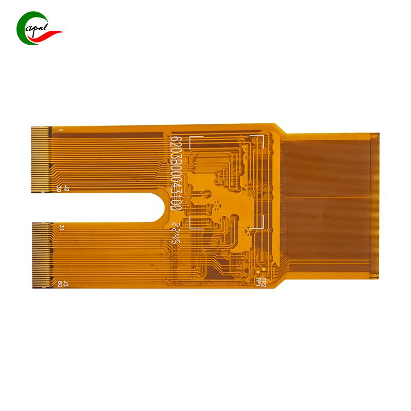
What Factors Determine the Flexibility Performance of Flexible PCBs?
Date: 2025-08-11
The ability of a flexible PCB to bend, twist, and fold repeatedly without failing is its most defining trait—but not all flexible PCBs are created equal. Some can withstand thousands of tight bends, while others crack after just a few. The difference lies in key factors that engineers carefully balance during design and manufacturing. Let’s break down what makes a flexible PCB truly "flexible."
The substrate is the flexible base that holds the circuit together, and its properties directly impact how well the PCB bends.
- Polyimide (PI): The gold standard for high-flex applications. PI substrates are heat-resistant, chemically stable, and retain their flexibility even after repeated bending. They’re ideal for devices like foldable phones or robotic arms, where durability under stress is critical.
- PET (Polyethylene Terephthalate): A cheaper alternative, but with lower flex life. PET works for low-stress uses (e.g., remote controls) but cracks faster under frequent bending or high temperatures.
- Thickness Matters: Thinner substrates (0.025mm to 0.1mm) bend more easily than thicker ones (0.1mm+). A PI substrate half as thick can often handle twice the number of bends before failing.
Copper carries electricity, but its form and thickness determine how well it survives bending.
- Rolled Copper vs. Electrodeposited Copper: Rolled copper is pressed into thin sheets, creating a uniform, ductile structure that bends without cracking. It’s the top choice for high-flex devices (e.g., fitness trackers with moving parts). Electrodeposited copper, built up through chemical processes, is stiffer and more prone to breaking under repeated stress—better for static or rarely bent circuits.
- Thin is Better for Flex: Thinner copper (12μm to 35μm) flexes more readily than thick layers (70μm+). Thick copper resists bending and can pull away from the substrate when folded, leading to failures.
How copper traces are arranged on the PCB is just as important as the materials themselves.
- Trace Direction: Traces running parallel to the bend axis (like lines along a fold) stretch and compress with each bend, fatiguing quickly. Traces routed perpendicular to the bend distribute stress evenly, doubling or tripling flex life.
- Trace Width and Spacing: Narrow traces (under 0.1mm) are more fragile, while overly wide ones add rigidity. Balanced width (0.1mm to 0.2mm) with ample spacing reduces stress concentration.
- Corner Radius: Sharp 90° corners act as stress "hot spots" where cracks start. Rounded corners (with a radius at least 3x the trace width) spread stress, preventing early failure—critical for devices like smartwatch hinges.
The materials that bond layers together affect both flexibility and durability.
- Adhesive Type: Epoxy-based adhesives are common but add stiffness. For ultra-flexible designs, "adhesive-free" PCBs use heat and pressure to bond layers, reducing bulk and improving bendability. These are key in medical implants, where every millimeter of flexibility counts.
- Number of Layers: Multi-layer flexible PCBs (with 2+ layers) are stiffer than single-layer ones. Each added layer increases thickness and reduces bendability, so engineers limit layers in high-flex applications (e.g., foldable displays).
Even the best-designed flexible PCB has limits, defined by its "minimum bend radius"—the smallest curve it can handle without damage.
- Design vs. Real-World Use: A PCB rated for a 1mm bend radius might fail if forced to bend to 0.5mm. Factors like temperature (cold makes materials stiffer) and humidity (moisture weakens adhesives) also reduce flex performance.
- Static vs. Dynamic Bending: A PCB bent once and held (static) lasts longer than one bent repeatedly (dynamic). Wearables or industrial robots need PCBs tested for dynamic flex—often 10,000+ bends—to ensure reliability.
Protective layers and stiffeners can either help or hinder flexibility.
- Cover Layer Material: Thin PI cover layers protect traces without adding much stiffness. Thicker PET covers, while cheaper, reduce bendability.
- Strategic Reinforcements: Small stiffeners (e.g., FR-4) add rigidity to connector areas but must be limited to non-bending zones. Overusing reinforcements in flex areas turns a "flexible" PCB into a rigid one.
In short, a flexible PCB’s ability to bend reliably depends on a delicate dance between materials, design, and usage. Engineers optimize these factors based on the device’s needs: a foldable phone demands rolled copper, perpendicular traces, and a thin PI substrate, while a rarely bent sensor might use PET with electrodeposited copper to cut costs. By tuning these variables, they ensure the PCB bends when it should—and lasts where it counts.
Founded in 2009, our company has deep roots in the production of various circuit boards. We are dedicated to laying a solid electronic foundation and providing key support for the development of diverse industries.
Whether you are engaged in electronic manufacturing, smart device R&D, or any other field with circuit board needs, feel free to reach out to us via email at sales06@kbefpc.com. We look forward to addressing your inquiries, customizing solutions, and sincerely invite partners from all sectors to consult and collaborate, exploring new possibilities in the industry together.
