
Date: 2026-07-14
You've definitely seen a circuit board before. Green, stiff, covered in copper traces and solder points. But there's a type of circuit board that doesn't use fiberglass, doesn't use epoxy — it uses ceramic as its base. It's not green, not flexible, not cheap — but it works where ordinary boards can't: high heat, high frequency, high power.
That's a ceramic PCB. Its core isn't the board itself — it's the ceramic substrate material. A ceramic PCB is a special process board where copper foil is directly bonded to the surface of a ceramic substrate like alumina (Al₂O₃), aluminum nitride (AlN), beryllium oxide (BeO), or silicon carbide (SiC) at high temperatures. In this guide, I'll explain what ceramic circuit board materials are, what types exist, where they're used, and why they're so expensive. Plain English, no fluff.
A regular circuit board (FR4) uses fiberglass cloth + epoxy resin — basically "plastic + glass." It's hard, but it can't handle high temperatures and doesn't conduct heat well. A ceramic circuit board uses inorganic, non-metallic compounds — the same family as ceramic tiles and porcelain, but much purer and much more powerful.
Key properties of ceramic substrates:
Excellent thermal conductivity: FR4 is 0.3-0.5 W/mK. Ceramic materials reach 24-180 W/mK — tens or even hundreds of times better.
Extreme temperature resistance: Ceramic substrates can handle over 800°C. FR4 starts softening at 150-180°C.
CTE matches silicon: Ceramic's coefficient of thermal expansion is very close to silicon chips. FR4 expands at a different rate — temperature changes crack solder joints.
Low signal loss at high frequencies: Ceramics have stable, low dielectric constant (Dk) and dissipation factor (Df), minimizing signal loss.
Excellent insulation: Ceramics can withstand breakdown voltages up to 20KV/mm.
Zero water absorption: Ceramics absorb 0% water — humidity has no effect.
The most common ceramic materials for PCBs are:
1. Alumina (Al₂O₃) — The Classic Workhorse
Alumina is the most popular ceramic substrate material in the electronics industry. Its thermal conductivity is about 24 W/mK — not as high as AlN, but already 50+ times better than FR4. Alumina offers great value, mature processes, and good mechanical strength. It's the default choice for most ceramic PCB applications.
2. Aluminum Nitride (AlN) — The Heat Dissipation King
AlN delivers 150-200 W/mK thermal conductivity, and its CTE perfectly matches silicon. With AlN substrates, you can use smaller heat sinks, fewer cooling components, higher power density, and lower overall system cost. The catch — expensive.
3. Beryllium Oxide (BeO) — The Extreme Performance Specialist
BeO hits 280-300 W/mK — almost like metal. But it's toxic and requires special handling. AlN is gradually replacing BeO.
| Feature | FR4 | Ceramic PCB |
|---|---|---|
| Substrate | Fiberglass + epoxy | Alumina/AlN ceramic |
| Thermal conductivity | 0.3-0.5 W/mK | 24-180 W/mK |
| Max operating temp | 130-180°C | >800°C |
| CTE match with silicon | Poor | Excellent |
| High-frequency performance | OK (struggles above 3GHz) | Excellent |
| Water absorption | Absorbs water | 0% absorption |
| Cost | Low | High (5-10×) |
| Best for | Most everyday electronics | High-temp, high-freq, high-power |
Ceramic PCBs aren't "better FR4" — they're specialty materials for applications where FR4 fails.
Making copper traces on ceramic is very different from FR4 etching. Several processes exist:
Thick Film: Conductive pastes are screen-printed onto the ceramic substrate and sintered at high temperature. Relatively simple, lower cost, good for production volumes.
Thin Film: Metal is deposited onto the ceramic in a vacuum using sputtering or evaporation. Traces can be as fine as 20-30μm with extremely high precision.
DPC (Direct Plated Copper): A thin seed layer is deposited using thin-film techniques, then copper is electroplated. Ideal for high-precision, high-alignment packaging.
DBC (Direct Bonded Copper): Copper foil is directly bonded to the ceramic at high temperature. Thick copper, high current capacity.
LTCC (Low Temperature Co-fired Ceramic): Multiple layers of ceramic green tape are stacked, printed with circuits, and co-fired together. Components can be embedded inside.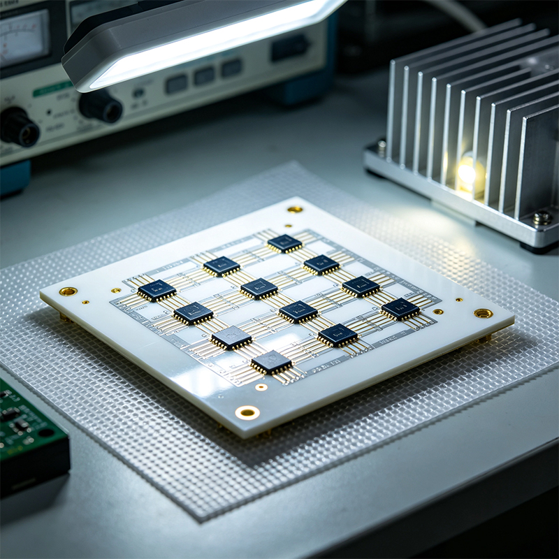
The ceramic PCB market is growing fast. They're used where ordinary boards can't survive:
Power Electronics: GaN devices are replacing silicon — they need better heat dissipation and temperature tolerance. Ceramic handles 300°C+.
RF and Communications: 5G base stations, RF devices — low signal loss and excellent heat dissipation are critical.
Automotive Electronics: High-power inverters, industrial automation — overheating leads to costly failures.
Aerospace and Defense: Extreme environments demand extreme reliability.
Medical Devices: High reliability, compact designs.
LED Lighting: High-power LEDs need exceptional heat dissipation.
Ceramic circuit board materials are the substrates used to make ceramic-based PCBs — most commonly alumina and aluminum nitride.
They're not "better" than FR4 — they're better suited for extreme environments: dozens of times better thermal conductivity, hundreds of degrees higher temperature tolerance, ultra-low high-frequency loss, and CTE that perfectly matches silicon chips. But they're expensive and complex to manufacture, so they only show up where ordinary boards can't handle the job.

Kaboer manufacturing PCBs since 2009. Professional technology and high-precision Printed Circuit Boards involved in Medical, IOT, UAV, Aviation, Automotive, Aerospace, Industrial Control, Artificial Intelligence, Consumer Electronics etc..


 English



 Wechat
 +86 13670210335
 +86 13670210335
 E-mail