
Date: 2026-08-03
You've definitely seen a circuit board before — green protective coating on top, white text and symbols underneath it, labels like “R1,” “C2,” “U3”. Have you ever wondered how that green layer and those white markings actually get onto the board?
The answer is — screen printing.
Screen printing (also called silkscreen printing) is one of the oldest and most widely used printing techniques in PCB manufacturing. Don't overthink it — the principle is the same as printing a design on a T-shirt: you use a mesh screen as a “stencil” and push ink through the mesh openings onto the board surface. The only difference is that on a PCB, you're not printing a design — you're printing protective layers and identification information. In this guide, I'll explain what PCB screen printing is, what it prints, how it works, and what's changing in the industry. Plain English, no fluff.
Screen printing does two big jobs on a circuit board:
Job #1: Solder Mask
That's the green (or red, blue, black) protective layer you see, commonly called “green oil.” It covers the copper traces, leaving only the pads exposed for soldering. Its job: prevent copper oxidation, prevent solder bridging during assembly, and provide electrical insulation.
Think of solder mask as the PCB's “raincoat” — once the copper traces put it on, they're protected from oxidation and shorts.
Job #2: Legend / Silkscreen Layer
That's the white text, symbols, outlines, and logos. “R1” tells you it's a resistor, “C2” tells you it's a capacitor, and a “+” next to a diode tells you which side is positive.
The legend layer doesn't conduct electricity — but the “navigation information” it provides is critical for assembly, testing, and repair. Without it, workers wouldn't know which component goes where.
The core process is simple — just four steps:
Step 1: Make the Screen
A fine mesh (usually polyester or stainless steel) is coated with photosensitive material to create the desired pattern. Where ink needs to go, the mesh is open; where it doesn't, the mesh is blocked.
Step 2: Registration and Printing
Align the screen over the PCB in exactly the right position. Then pour specialized ink onto one end of the screen and use a squeegee to push it evenly across — the ink is forced through the mesh openings and transferred onto the PCB surface. If the alignment is off, the text comes out crooked.
Step 3: Pre-cure
The printed board goes through a low-temperature bake to set the ink.
Step 4: Final Cure
A high-temperature bake (around 150°C) fully cures the ink, permanently bonding it to the board surface.
The solder mask process is similar, but it uses solder mask ink and involves additional exposure and development steps after printing to form the final protective layer.
PCB screen printing comes in three flavors, depending on precision and volume:
1. Manual Screen Printing — The Cheapest, Most Traditional
A nylon mesh stencil and a hand-held squeegee, all done by hand. The advantage is simple: cheap. For small prototype runs, the equipment cost is almost zero. The downside is low precision and operator-dependent — it only works for line widths above 0.178mm (7mil) and registration tolerance of ±0.127mm (5mil). Fine text is impossible, and it doesn't scale to high volume.
2. LPI (Liquid Photo Imaging) — The Industry Standard
LPI is the dominant method in modern PCB manufacturing. Instead of printing directly, a photosensitive epoxy ink is coated onto the board, then exposed to UV light through a film photomask — exposed areas harden, and unexposed areas are washed away in developer solution.
LPI is far more precise than manual printing — line widths down to 0.15mm and character heights down to 0.8mm. It's fast, accurate, and perfect for high-volume production.
3. Digital Inkjet Printing (DLP) — The Newcomer
This is an emerging technology. It prints ink directly onto the PCB surface like a desktop printer — no screen required. Precision is extremely high — line widths down to 0.05-0.08mm. Switching boards just means changing a program — no new screen needed. The downside: equipment is expensive and adoption is still limited.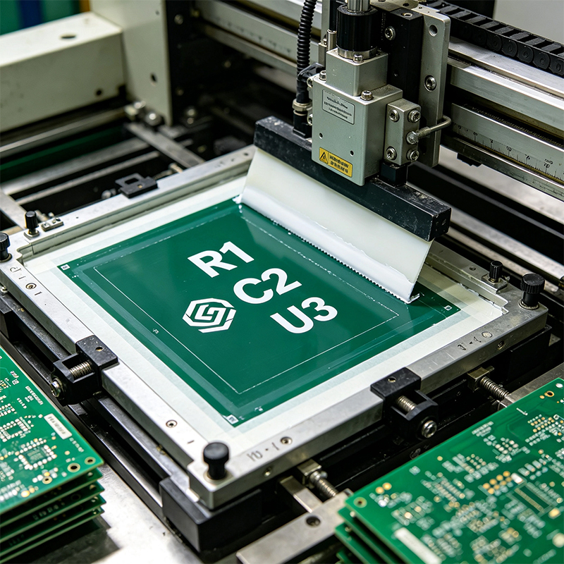
PCB screen printing inks are nothing like regular printing inks. They have to be heat-resistant (to survive reflow soldering), chemically resistant, strongly adhesive, and non-conductive.
The most common ink for the legend layer is epoxy ink, and the most common color is white — it contrasts best against the green solder mask. Black, yellow, and other colors are also available.
Solder mask uses photosensitive solder mask ink, available in thermal-curing and UV-curing types. Green is the absolute dominant color — it's easiest on the eyes and the cheapest.
Silkscreen design seems simple, but there are several rules you must follow:
Keep off pads: Silkscreen ink is non-conductive — if it covers a pad, soldering won't work. Keep at least 0.15mm clearance from pads.
Keep off vias and test points: These need electrical contact — they can't be covered by ink.
Don't make text too small: Character height should be at least 0.8mm and line width at least 0.15mm — anything smaller will blur together.
Place near components, not on them: Silkscreen should be close to the component it labels, but not covered by the component after assembly.
Traditional screen printing has been around for decades, but it has a clear limitation — precision bottlenecks. Screens stretch, squeegee pressure varies, and ink flow changes, making it hard to consistently achieve line widths below 0.1mm. For high-density BGAs and tiny components like 0201 or 01005, the reference designators often overlap, break, or blur.
That's why more PCB manufacturers are switching to digital inkjet printing — higher precision, more flexibility, no screen-making required.
PCB screen printing is the process of using a mesh screen to push ink onto a circuit board surface. It does two big jobs in PCB manufacturing: printing the solder mask (protecting copper traces) and printing the legend layer (providing identification information). It comes in three flavors — manual, LPI, and digital inkjet — each with different precision and cost trade-offs.

Kaboer manufacturing PCBs since 2009. Professional technology and high-precision Printed Circuit Boards involved in Medical, IOT, UAV, Aviation, Automotive, Aerospace, Industrial Control, Artificial Intelligence, Consumer Electronics etc..


 English



 Wechat
 +86 13670210335
 +86 13670210335
 E-mail