
Date: 2026-08-03
You're designing an electronic product. Maybe an industrial controller, a medical device, an automotive sensor, or an AI edge computing module. You spent weeks on the schematic, selected every component, and received the finished boards. But have you ever thought about how that bare board went from raw materials to a finished product in your hands?
A circuit board goes through dozens or even hundreds of process steps from design files to finished product. Every step has strict process controls and quality standards. In this guide, I'll walk you through the complete PCB manufacturing process — from design files to finished boards. Plain English, no fluff.
PCB manufacturing doesn't start with someone "reading a drawing" on the factory floor. It starts with receiving and reviewing design files.
The design files you submit typically include: Gerber files (defining every layer — copper, solder mask, silkscreen), drill files (defining hole positions and sizes), stackup (defining layer count and material sequence), and a BOM if assembly is required.
DFM (Design for Manufacturing) review is the first quality checkpoint. Engineers check your design: Is trace width sufficient? Is clearance adequate? Is the aspect ratio reasonable? Is the material selection correct? If there are issues, they're flagged before production starts. This step catches problems before they become expensive physical defects.
A key trend in 2026 is IPC-2581 v4.0 and other smart data formats gradually replacing traditional Gerber files. IPC-2581 packages all manufacturing data into a single file, reducing errors during file conversion.
The first physical step is selecting the right substrate and cutting it to production size.
The substrate is the circuit board's "skeleton" — all copper traces and components sit on it. Common substrates include:
FR4 (fiberglass epoxy) : The most common substrate, covering 70-80% of the global PCB market. Cheap, stable, and easy to process.
Polyimide (PI) : The soul of flexible circuits — heat-resistant and bendable.
Rogers/PTFE: High-frequency low-loss materials for 5G, radar, and other high-frequency applications.
Once the substrate is selected, it's cut to standard production size using automated cutting machines. Factories have minimum and maximum processing sizes based on equipment capabilities.
For multi-layer boards, manufacturing starts with inner layer patterning.
Step 1: Apply Dry Film (Photoresist)
A photosensitive dry film is laminated onto the copper surface. Dry film is a light-sensitive polymer film that covers the copper like plastic wrap.
Step 2: Exposure (LDI – Laser Direct Imaging)
A computer-controlled laser exposes the circuit pattern onto the dry film. Exposed areas harden; unexposed areas remain soluble. LDI is gradually replacing traditional film-based exposure for higher precision and faster throughput.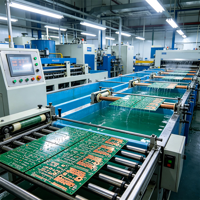
Step 3: Development and Etching
The board goes into a developer solution — unexposed dry film dissolves away, exposing the copper underneath. Then an etchant removes the exposed copper. The remaining copper is your circuit pattern.
Etching must be precisely controlled — over-etching makes traces thin and fragile; under-etching leaves residual copper that can cause shorts.
Step 4: AOI (Automated Optical Inspection)
After etching, AOI checks inner layers for opens, shorts, and defects. AOI uses high-resolution cameras to compare the board to a reference image.
Once all inner layers are patterned, they must be stacked and pressed into a single board.
The stackup is: inner layer cores + prepreg + copper foil + prepreg + inner layer cores… . Prepreg is fiberglass cloth impregnated with resin — it melts, flows, and cures under heat and pressure, bonding the layers together.
The stack goes into a high-temperature, high-pressure press — heated to 180-200°C and pressed to laminate all layers into a single board.
Lamination is one of the most critical steps in PCB manufacturing. Interlayer alignment precision directly determines yield — misregistration beyond 0.05mm means vias miss pads.
For rigid-flex boards, lamination is even harder — rigid and flex sections must be laminated into one piece, and the transition zone is the most fragile point. After lamination, precision depth routing removes excess rigid material to expose the flex layers.
After lamination, the next step is drilling.
There are two types:
Mechanical drilling: For through-holes — holes that go all the way from top to bottom. Minimum hole diameter is typically around 0.15mm.
Laser drilling: For blind and microvias — holes that only connect adjacent layers. Minimum diameter can go down to 0.075mm or less.
Drilling precision is critical — misaligned holes miss pads; crooked holes create rough walls. In 2026, laser drilling is the standard for HDI boards.
After drilling, copper is plated into the hole walls to connect different layers.
The plating process:
Electroless copper deposition: A thin layer of copper (about 0.5-1μm) is chemically deposited on the hole walls as a conductive seed layer.
Electroplating: The board goes into an electroplating bath — copper deposits on the hole walls and board surface.
Plating thickness must be precisely controlled — too thin and current can't pass through; too thick and holes may plug. In multi-layer and HDI boards, plating uniformity directly determines microvia reliability.
After plating, outer layer circuitry is patterned on the outer copper layers.
The process is the same as inner layers: apply dry film → expose → develop → etch → strip. But outer layers also require impedance control — high-speed signal trace impedance must precisely match the design value.
After outer layer patterning, the board gets solder mask.
Solder mask is the green (or red, blue, black) protective layer you see — commonly called "green oil". It covers the copper traces, leaving only the pads exposed for soldering. Its job: prevent copper oxidation, prevent solder bridging, and provide insulation.
After solder mask, silkscreen is printed onto the board — those white letters and symbols. "R1", "C2", "U3" — telling you which component goes where.
The exposed pads need a surface finish to protect the copper and ensure solderability.
Common options include:
HASL (Hot Air Solder Leveling) : Cheapest, good solderability, but uneven surface.
ENIG (Electroless Nickel Immersion Gold) : Ultra-flat, long shelf life, ideal for fine-pitch and BGA.
OSP (Organic Solderability Preservative) : Very cheap, flat, but short shelf life.
Immersion Silver / Immersion Tin: In between.
After manufacturing, every board goes through 100% electrical testing.
Testing checks for two things: opens (broken traces) and shorts (unintended connections) . The two main methods are:
Flying probe test: Movable probes contact test points one by one — ideal for low volume.
ICT (In-Circuit Test) : A bed-of-nails fixture tests all points simultaneously — ideal for high volume.
After electrical testing, boards go through final visual inspection (FQC) — checking solder mask for bubbles, silkscreen for clarity, edges for burrs. Only after passing all checks are they packaged and shipped.
A circuit board goes through engineering review, substrate preparation, inner layer imaging, lamination, drilling, plating, outer layer imaging, solder mask, silkscreen, surface finish, and testing — over a dozen major process steps.
Every step has strict quality controls — AOI for inner layers, X-Ray for drilling, flying probe and ICT for electrical testing, FQC for visual inspection.
We are a custom manufacturer of flexible PCBs, rigid-flex boards, HDI high-frequency boards, and full PCBA services — from DFM review to finished products, all in-house. Have a PCB manufacturing need? Send us your design files — we'll get back to you with a DFM report and quote within 24 hours.

Kaboer manufacturing PCBs since 2009. Professional technology and high-precision Printed Circuit Boards involved in Medical, IOT, UAV, Aviation, Automotive, Aerospace, Industrial Control, Artificial Intelligence, Consumer Electronics etc..


 English



 Wechat
 +86 13670210335
 +86 13670210335
 E-mail