
Date: 2026-07-09
You know how chips are made — hundreds of them are etched onto a silicon wafer, then cut into individual black squares and sent to a packaging factory to get "dressed." But what if you could put the "clothes" on before cutting? So that each chip comes out already packaged, ready to use, without an extra packaging step.
That's wafer-level packaging.
Its full name is Wafer-Level Packaging (WLP) . It's not the traditional "cut first, package later" approach — it's package first, cut later. All packaging steps are done on the wafer, and only at the very end are the chips singulated. In this guide, I'll explain what wafer-level packaging is, what types exist, how it's made, and where it's used. Plain English, no fluff.
Traditional packaging cuts the wafer into individual dies first, then packages each one separately — each chip gets its own housing and leads. This is "cut first, package later".
Wafer-level packaging flips the order: before the wafer is cut, all packaging steps are done on the entire wafer — routing, solder balls, insulation layers, everything. Only after that is the wafer diced into finished, packaged chips.
Think of a pizza. Traditional method: cut it into slices first, then box each slice individually. Wafer-level packaging: box the whole pizza first, then cut it — much more efficient and cheaper.
The resulting chip is almost exactly the same size as the bare die itself — this is called a chip-scale package (CSP) . Much smaller than traditional packages — perfect for phones, watches, and earbuds where every millimeter counts.
Here's a quick comparison:
| Feature | Traditional Packaging | Wafer-Level Packaging |
|---|---|---|
| Order | Cut first, then package | Package first, then cut |
| Package size | Much larger than die | Nearly the same as die |
| Signal path | Long (through lead frames or wires) | Short (direct to PCB) |
| High-frequency performance | Moderate | Excellent (30-60% lower inductance) |
| Cost at volume | Higher (handled individually) | Lower (batch processed) |
| Best for | All chip types | High-density, compact, high-performance chips |
Wafer-level packaging comes in two main flavors: Fan-in and Fan-out.
Fan-In WLP
This is the original wafer-level packaging. All I/O connections are routed within the footprint of the die. All solder balls sit within the chip's "territory."
The advantage: the package is exactly the same size as the die — the smallest package possible. The limitation: the die's surface area limits how many I/O connections you can have.
Fan-in WLP is used for low pin-count chips — power management ICs, sensors, Bluetooth chips, and more. The iPhone 5 uses at least 11 different WLP chips.
Fan-Out WLP
Fan-in squeezes everything inside the chip. Fan-out places the chip into a "reconstituted" wafer and extends routing beyond the chip's boundaries.
Think of it like this: Fan-in is a small apartment — everything is packed inside. Fan-out is knocking down a wall — you get extra space for more "furniture." Fan-out supports more I/O connections, making it suitable for more complex chips.
Fan-out WLP is used in high-performance computing, automotive electronics, and 5G communications — applications that need lots of pins and high performance.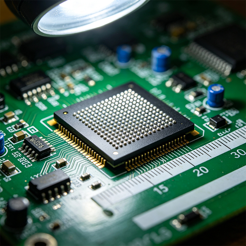
The manufacturing process for wafer-level packaging shares many similarities with chip fabrication itself. Here are the core steps:
Step 1: Apply Dielectric Layer
A layer of insulating material (typically polyimide PBO or PI) is coated on the wafer surface. Photolithography opens windows where needed, exposing the chip's pads.
Step 2: Redistribution Layer (RDL)
The chip's original pads might be scattered around the perimeter, making them hard to connect directly to a PCB. RDL re-routes these connections — using sputtering and electroplating to create new metal traces that "move" the pads to more convenient locations.
Step 3: Under Bump Metallization (UBM)
At the end of each RDL trace, a transition metal layer (UBM) is created to prepare for solder balls.
Step 4: Ball Mounting
Solder balls are placed on the UBM pads. These balls become the chip's "feet" for connecting to the outside world.
Step 5: Singulation
Only after all packaging steps are complete is the wafer diced into individual chips.
The core logic: all packaging operations are done in batch on the wafer, and only at the very end is it cut. That's the fundamental reason wafer-level packaging is so efficient.
1. Small
The package is nearly the same size as the die itself. Smartphone motherboards can fit hundreds of components — thanks to this technology.
2. Great Signal Performance
Shorter signal paths mean lower parasitic inductance. For 5G, Wi-Fi, and high-speed data, signal quality is everything.
3. Good Heat Dissipation
Chips connect directly to the PCB through solder balls — short thermal path. Heat dissipates faster.
4. Lower Cost (at Volume)
All packaging steps are done in batch on the wafer, spreading the cost across every chip.
1. Limited I/O Count (Fan-In)
Fan-in WLP's I/O count is limited by die size. Small die, lots of pins — Fan-in won't work.
2. CTE Mismatch
Silicon and PCB expand at different rates with temperature. Solder balls experience stress.
3. PCB Design Requirements
WLCSP ball pitch is typically under 0.5mm. PCBs need high-precision pads and traces.
4. Difficult Rework
Once a WLP chip is soldered down, removing and re-soldering it is extremely difficult — the balls are too small.
5. Testing Challenges
Wafer-level packaging requires testing at the wafer stage. If there are bad chips on the wafer, packaging costs are wasted.
Wafer-level packaging is a technology where all packaging steps are done on the entire wafer before it's diced.
Its defining feature is package first, cut later — the exact opposite of traditional "cut first, package later." The resulting chip is nearly the same size as the bare die, with excellent signal quality, good heat dissipation, and low cost at volume.
It comes in two types: Fan-in and Fan-out. Fan-in keeps all connections within the chip's footprint — suitable for simpler chips. Fan-out extends connections beyond the chip — suitable for complex, high-performance chips.
Phones, watches, earbuds, 5G devices, automotive electronics — every smart device around you has WLP chips working quietly inside. They're not flashy, but they're one of the key technologies that make electronics smaller and more powerful.

Kaboer manufacturing PCBs since 2009. Professional technology and high-precision Printed Circuit Boards involved in Medical, IOT, UAV, Aviation, Automotive, Aerospace, Industrial Control, Artificial Intelligence, Consumer Electronics etc..


 English



 Wechat
 +86 13670210335
 +86 13670210335
 E-mail