
Date: 2025-07-10
Discover a comprehensive guide to double-layer flexible printed circuit board (PCB) design, layout, types, prototyping, manufacturing, and applications. Gain insight into the importance of proper design, Kaboer’s expertise, and future trends in the industry.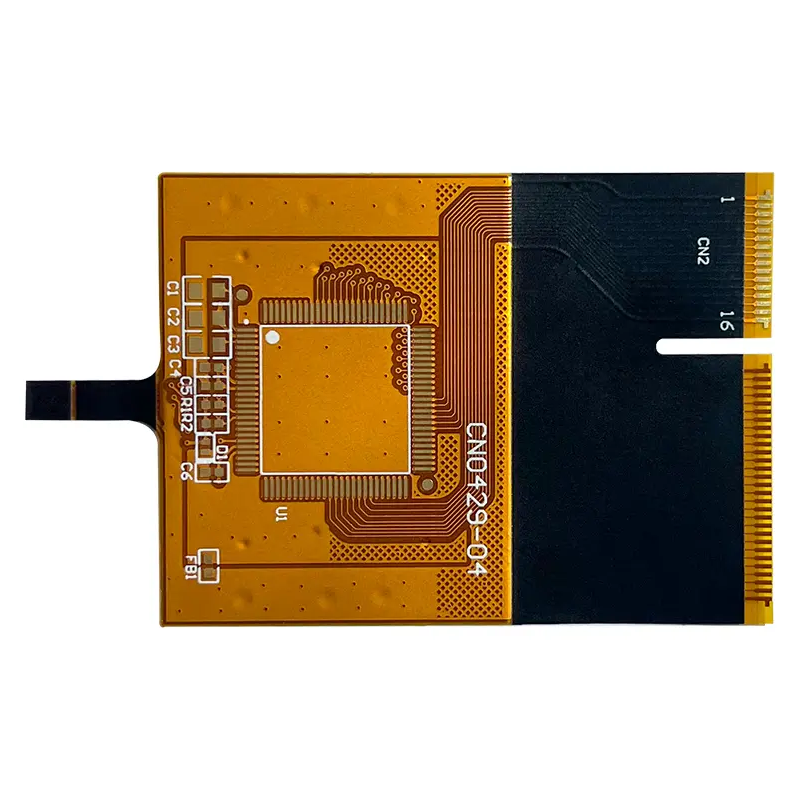
In the field of electronics, the demand for flexible and compact circuits has been growing. Double-layer flexible printed circuit boards (PCBs) have emerged as a key solution to meet this need. These boards offer the flexibility and space-saving advantages of flexible PCBs while providing additional layers for more complex circuits.
The design, layup, type, prototyping, manufacturing and application of double-layer flexible PCB are key links that directly affect the performance and reliability of electronic devices. Understanding these elements is critical for engineers, designers and manufacturers to realize the full potential of double-layer flexible PCBs.
Kaboer has been a leading supplier of double layer flexible PCB solutions for over 16 years. With a strong focus on innovation and quality, Kaboer has become a trusted partner for businesses seeking high-performance dual-layer flexible PCBs.
A two-layer flexible PCB consists of two conductive layers separated by a flexible dielectric material. This unique structure increases circuit density and improves signal integrity while maintaining flexibility.
The advantages of double-layer flexible PCBs include light weight, space-saving design, excellent flexibility and high reliability. These properties make it ideal for applications in industries such as aerospace, medical devices, automotive and consumer electronics.
Proper design and layout are critical to ensuring the mechanical and electrical integrity of a double-layer flexible PCB. Attention to detail during the design and layout process is critical to avoid problems such as signal interference, impedance mismatch and mechanical failure.
Designing a two-layer flexible PCB requires careful consideration of factors such as signal routing, layer stacking, impedance control, and thermal management. These considerations are critical to achieving optimal performance and reliability.
The design process is influenced by factors such as circuit complexity, operating environment, and specific requirements of the end application. Understanding these factors is critical to creating a design that meets the required performance standards.
Best practices for designing dual-layer flex PCBs include utilizing flex PCB-capable design software, conducting thorough signal integrity analysis, and working closely with the manufacturing team to ensure the design is manufacturable.
There are many types of double-layer flexible PCBs, including rigid-flex boards, engraved flex boards, and multi-layer flex boards. Each type offers unique advantages and is suitable for specific applications based on factors such as space constraints, mechanical requirements and cost considerations.
Comparing different types of double-layer flexible PCBs based on factors such as bend radius, number of layers, and material properties can help select the most appropriate type for a specific application. Understanding these comparisons is critical to making informed design decisions.
Selecting the correct type of double-layer flexible PCB based on specific project requirements is critical to achieving the required performance, reliability and cost-effectiveness. Factors such as form factor, mechanical constraints, and environmental conditions play an important role in this selection process.
Prototyping is a critical stage in double-layer flex PCB development as it allows the design to be tested and verified before mass production. Prototyping helps identify and solve potential problems early in the development cycle.
The prototyping process involves steps such as design verification, material selection, prototype board fabrication, and thorough testing and evaluation. Each step is critical to ensuring the functionality and reliability of the prototype.
Common challenges in prototyping dual-layer flexible PCBs include material selection, manufacturing tolerances, and signal integrity issues. Addressing these challenges requires close collaboration between design, manufacturing and test teams to find effective solutions.
The manufacturing process of double-layer flexible PCB involves steps such as material preparation, imaging, etching, lamination, drilling, plating and final assembly. Each step requires precision and attention to detail to ensure the quality and reliability of the finished board.
Advanced manufacturing technologies such as laser drilling, controlled impedance processing and automated assembly play a vital role in the production of high-quality double-layer flexible PCBs. Understanding these technologies is critical to achieving consistent and reliable manufacturing results.
Strict quality control measures and testing protocols are critical to ensure the reliability and performance of double-layer flexible PCBs. Testing of factors such as impedance, signal integrity and mechanical durability is critical to identifying and resolving any manufacturing defects.
Double-layer flexible PCBs are widely used in various industries, including aerospace, medical devices, automotive, telecommunications and consumer electronics. Their flexibility, lightweight design and high reliability make them suitable for a variety of applications.
Case studies demonstrate the successful use of double-layer flexible PCBs in real-world projects, providing valuable insights into their performance and reliability in different industry environments. These case studies demonstrate the versatility and effectiveness of dual-layer flexible PCBs in meeting specific application requirements.
With the continuous advancement of materials, manufacturing processes and design technology, the future of double-layer flexible PCB is full of hope. Potential new applications in areas such as wearable electronics, IoT devices, and flexible displays provide exciting opportunities for the continued growth of double-layer flexible PCB technology.
A thorough understanding of double-layer flexible PCB design, layout, type, prototyping, manufacturing, and application is critical to achieving optimal performance and reliability of electronic devices.
Kaboer’s 16 years of expertise and commitment to innovation and quality make it a trusted partner for businesses seeking high-performance dual-layer flexible PCB solutions. Kaboer’s expertise and dedication to customer satisfaction have made it a leading supplier in the industry.
For further inquiries and partnership opportunities in double layer flexible PCB development and production, Kaboer welcomes collaboration with businesses and organizations seeking reliable and innovative PCB solutions.
In summary, the design, layout, type, prototyping, manufacturing and application of double-layer flexible PCBs are key aspects that require careful consideration and expertise. With Kaboer’s extensive experience and commitment to quality, companies can leverage the potential of double-layer flexible PCB technology to drive innovation and success in their electronic products and applications.
![]()
Kaboer manufacturing PCBs since 2009. Professional technology and high-precision Printed Circuit Boards involved in Medical, IOT, UAV, Aviation, Automotive, Aerospace, Industrial Control, Artificial Intelligence, Consumer Electronics etc..


 English


 Wechat
 +86 13670210335
 +86 13670210335
 E-mail