Date: 2026-01-19
You're designing a new product. The specs call for something powerful yet compact—maybe a wearable health monitor, a miniaturized IoT sensor, or the next-gen router. Your circuitry is complex, but the board real estate is tight. You know a standard double-sided board won't cut it; you need to go multilayer.
This is where things get interesting. When you move to 4, 6, or 12-layer boards, you face a fundamental routing problem: how do you connect signals between the inner layers without wasting precious space on the outer ones?
Enter the unsung hero of high-density design: the Blind Via.
Think of a standard through-hole via like a public elevator that goes from the roof all the way to the basement, stopping at every floor. It's useful but takes up space on every single level of your building (your PCB).
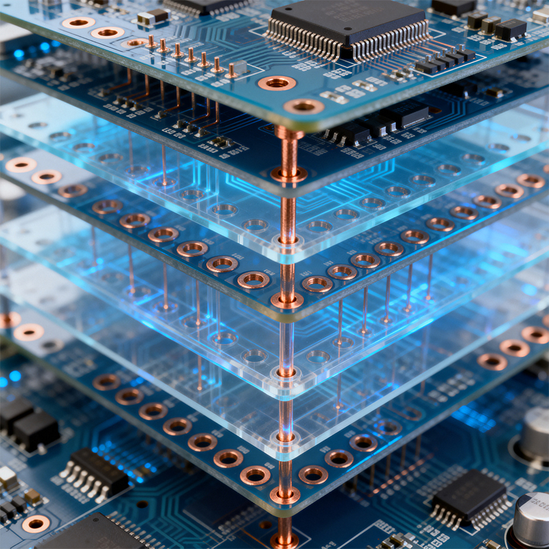
A Blind Via, in contrast, is like a private staircase connecting only two specific floors—say, the penthouse to the floor just below it. It starts on an outer layer (top or bottom) and terminates at an inner layer, without going all the way through the board. It’s a precise, space-saving connection.
So why go through the extra manufacturing step? Because blind vias solve specific headaches in modern electronics:
They Free Up Precious Real Estate: This is the biggest win. By not penetrating the entire board, they don't occupy space on layers they don't need to. This leaves more room on inner and opposite outer layers for routing other critical traces. You can pack more functionality into a smaller area.
They Enable Denser BGA Fanouts: High-pin-count chips (like modern BGAs) are a routing nightmare. Blind vias allow you to escape signals from the dense ball grid directly to the inner layers right beneath the chip, making routing possible without needing an enormous board.
They Can Improve Signal Integrity: For high-speed signals, a via is not just a hole; it's an "antenna stub." A through-hole via creates a long stub that can reflect signals and degrade performance. A blind via, being shorter, minimizes this stub effect, leading to cleaner signals—critical for RF, high-speed digital, and memory applications.

They’re not for every project. Think of them as a specialized tool. You'd consider them when:
Your component density is extremely high (think smartphones, advanced modules).
You're working with fine-pitch BGAs where escape routing is the primary constraint.
The design has serious layer count and size limitations ("make it 30% smaller").
Signal integrity at high frequencies is a non-negotiable requirement.
Nothing in engineering is free. Before specifying blind vias, be aware:
Cost Impact: The process is more complex than standard drilling, requiring precise laser drilling and additional lamination steps. This increases board cost, often significantly.
Lead Time: The added manufacturing steps can extend production time.
Design Complexity: Your PCB layout software and your fabricator's design rules need to support them. The stack-up planning becomes more critical.
This is the crucial part. Successfully manufacturing a board with blind vias is a litmus test for a PCB fabricator's capabilities. It requires precision equipment (like laser drills) and deep process control.
This is where partnering with an integrated PCBA manufacturer like Kaboer offers a distinct advantage. Because we control both the PCB fabrication and the assembly in our own Shenzhen factory, the entire process is seamless.
For you, this means:
No Finger-Pointing: There's no "the board house made the vias wrong" vs. "the assembler damaged them" debate. One team owns the entire process from drilling to soldering.
Optimized for Assembly: We understand how via design affects solder paste flow and thermal management during reflow, and can advise on optimal designs.
Direct Feedback Loop: Our engineering teams for fabrication and assembly work side-by-side. If there's a potential issue with your blind via design for manufacturability (DFM) or assembly, we catch it and suggest solutions early.
Blind via PCBs are a powerful enabling technology for the miniaturized, high-performance electronics that define today's market. They aren't a default choice, but a strategic one for overcoming specific design challenges.
When your project demands that level of sophistication, choosing a manufacturing partner with proven, in-house expertise in advanced PCB fabrication and assembly isn't just a good idea—it's essential for bringing your complex design to life reliably and efficiently.
Kaboer manufacturing PCBs since 2009. Professional technology and high-precision Printed Circuit Boards involved in Medical, IOT, UAV, Aviation, Automotive, Aerospace, Industrial Control, Artificial Intelligence, Consumer Electronics etc..