Date: 2025-12-19
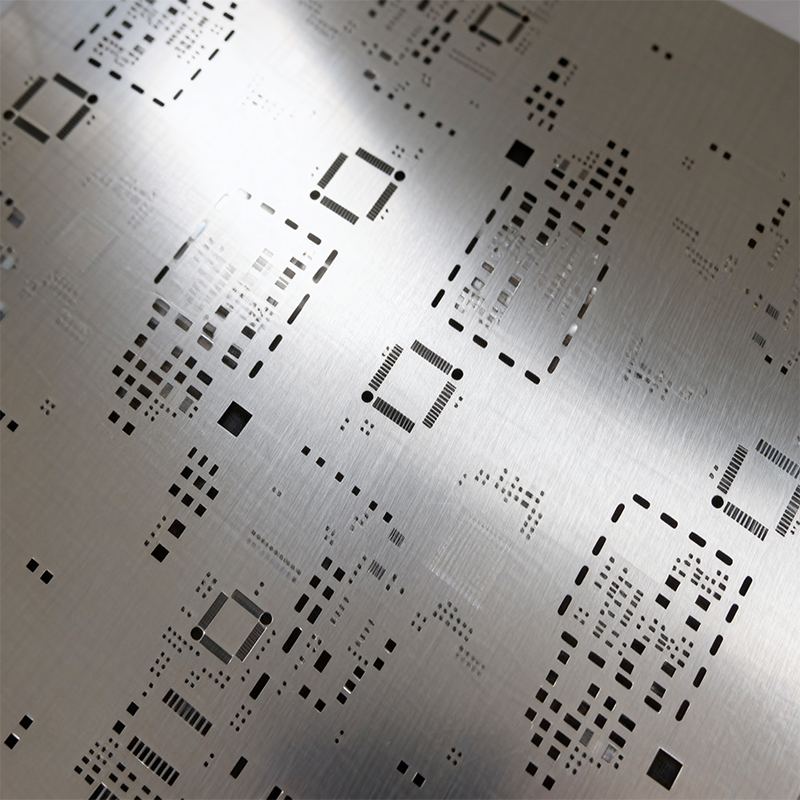
A circuit board stencil, also known as a solder paste stencil, is a thin sheet of stainless steel or polyester with laser-cut openings that correspond to the solder pad locations on a printed circuit board (PCB). During surface mount technology (SMT) assembly, solder paste is applied through these openings onto the PCB pads, ensuring precise and consistent deposition before component placement.
High-quality stencils ensure accurate solder paste volume and placement, reducing defects like bridging, insufficient solder, or misalignment.
Properly designed stencils speed up the printing process, allowing for faster throughput in manufacturing lines.
By minimizing rework and improving first-pass yield, reliable stencils directly lower assembly costs.

The most common type, offering excellent durability and precision for high-volume production.
Created through nickel plating, these provide superior accuracy for ultra-fine-pitch components.
Feature a smooth, non-stick surface that reduces solder paste adhesion and improves release characteristics.
Combine different technologies to optimize performance for mixed-component boards.
Properly designed aperture walls with optimal taper ratios ensure clean solder paste release.
Typically ranging from 0.1mm to 0.15mm (4-6 mil), thickness selection depends on component pitch and paste requirements.
Electropolished or nano-coated surfaces improve paste release and reduce cleaning frequency.
Durable frames with proper tension maintenance ensure consistent printing performance.
Different components (from 01005 chips to BGAs) require tailored aperture designs on the same stencil.
Humidity and temperature affect solder paste behavior and should influence stencil specifications.
Low-quality stencils lead to higher defect rates, negating any initial cost savings.
Regular cleaning and proper storage extend stencil life and maintain print quality.
At Kaboer, we understand that quality circuit board stencils are just one element of successful electronics manufacturing. As a professional PCBA manufacturer based in Shenzhen, China, we operate our own factory equipped with advanced SMT lines and inspection systems.
Our expertise extends beyond stencil selection to complete manufacturing solutions:
In-House Stencil Fabrication: We produce custom laser-cut stencils optimized for your specific PCB designs
DFM Analysis: Our engineering team provides design feedback to improve manufacturability
Full Turnkey PCBA: From component sourcing to final assembly and testing
Quality Assurance: Comprehensive inspection at every production stage
Located in the heart of China's electronics industry, we combine manufacturing efficiency with international quality standards to serve global electronics brands.
Whether you're establishing a new production line or improving existing processes, remember that the circuit board stencil is not just a tool but a critical determinant of assembly quality. Partnering with experienced manufacturers who understand the interplay between stencil design, solder paste, and equipment can significantly impact your production outcomes.
By focusing on precision stencils as part of a holistic manufacturing approach, electronics manufacturers can achieve higher yields, better product reliability, and ultimately, greater customer satisfaction in today's competitive marketplace.
Kaboer manufacturing PCBs since 2009. Professional technology and high-precision Printed Circuit Boards involved in Medical, IOT, UAV, Aviation, Automotive, Aerospace, Industrial Control, Artificial Intelligence, Consumer Electronics etc..