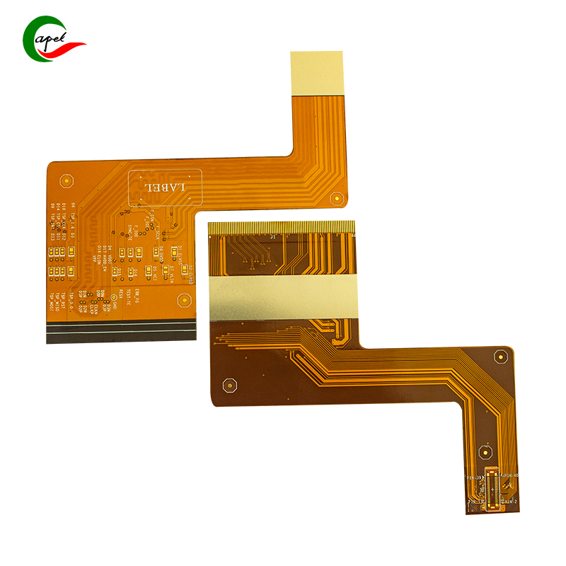
Common Issues in Flexible PCB Circuit Design
Date: 2025-08-10
Flexible PCBs have revolutionized how electronics fit into tight, dynamic spaces, but their unique design demands careful attention to avoid costly mistakes.
From material mismatches to wiring errors,even small oversights can derail performance. Here’s a breakdown of the most frequent pitfalls engineers face—and how they impact real-world use.
The flexibility of these PCBs relies heavily on their core materials, and choosing the wrong ones is a recipe for failure.
Substrate missteps: Polyimide (PI) is a workhorse for high-heat environments (like car engines), handling temps up to 300°C. But using cheaper PET (polyethylene terephthalate) in the same settings is disastrous—PET melts around 120°C, causing the board to warp or short. Conversely, overspending on PI for low-stress devices (e.g., remote controls) wastes resources without added benefit.
Copper type errors: Rolled copper, with its superior bendability, is a must for foldable phones or robotic arms that flex thousands of times. Electrodeposited copper, while smoother for tiny circuits, cracks easily under repeated bending. Using the latter in high-flex areas leads to 断线 (broken traces) and intermittent connectivity.
Flexible PCBs bend, so their trace paths and spacing need to account for mechanical stress—something rigid PCB designers often overlook.
Wrong trace direction: Traces running parallel to the bend axis (like lines along a foldable phone hinge) get stretched on the outer curve and crushed on the inner curve. This leads to early fatigue and 断裂 (breaks). The fix? Route traces perpendicular to the bend to distribute stress evenly.
Tight spacing or thin traces: Shrinking trace width below 0.1mm boosts resistance, causing signal lag or overheating. Similarly, spacing traces too close (under 0.1mm) invites short circuits, especially in high-humidity environments where moisture bridges gaps. This is a common issue in compact wearables, where designers prioritize size over safety.
Via overload: Vias (holes connecting layers) weaken flexibility. Clustering them in bend zones or using undersized vias creates stress points that crack during use—critical failures in medical devices like pacemakers, where reliability is life-or-death.
Flexible PCBs thrive under motion, but pushing their physical limits dooms them to failure.
Bending too sharply: Every flexible PCB has a minimum bend radius (e.g., 0.5mm for a 0.1mm-thick PI board). Folding it tighter—say, into a right angle—rips the substrate and snaps copper traces. This plagues foldable laptops when hinges are forced beyond design specs.
Bad mounting: Securing the PCB with a single screw or weak adhesive lets it vibrate (common in car dashboards), fatiguing traces until they break. Over-tightening screws also crushes the substrate, damaging internal layers.
No stress relief: Sharp 90° corners in traces act like stress magnets. Without rounded bends or buffer zones, these spots crack first in devices with constant motion, like smartwatch crowns or drone motors.
Flexible PCBs aren’t just about bending—they must handle heat and high-frequency signals too.
Poor heat management: PI and PET conduct heat poorly compared to rigid FR-4. Placing power-hungry components (like LEDs or chips) without large copper heat sinks traps heat, melting adhesives or warping the board. This is a frequent issue in LED strip lights, where overheating shortens lifespans.
High-frequency signal loss: Flexible substrates have unstable dielectric constants (Dk) that shift with bending or temperature. This throws off impedance matching in 5G modems or radar systems, causing signal bounce or dropout. Skipping shielding or using unoptimized trace lengths exacerbates the problem.
Even great designs fail if they ignore factory capabilities.
Unrealistic specs: Demanding 0.05mm traces when a manufacturer’s minimum is 0.075mm leads to inconsistent etching—some traces short, others break. Similarly, tiny coverlay windows (under 0.2mm) cause alignment errors, leaving copper exposed to corrosion.
Mismatched stiffeners: Stiffeners (like FR-4 or steel) add rigidity to connectors but backfire if oversized. They restrict bending, creating stress at the stiffener edge that peels layers apart—ruining PCBs in automotive sensors.
Designing flexible PCBs means balancing flexibility with durability, electrical performance with manufacturability. Avoiding these pitfalls starts with understanding the board’s intended use: a foldable phone needs rolled copper and rounded traces, while a high-heat sensor requires PI substrate and heat sinks. By prioritizing both mechanical and electrical needs, engineers can unlock the full potential of these versatile circuits—without the headaches.
Founded in 2009, our company has deep roots in the production of various circuit boards. We are dedicated to laying a solid electronic foundation and providing key support for the development of diverse industries.
Whether you are engaged in electronic manufacturing, smart device R&D, or any other field with circuit board needs, feel free to reach out to us via email at sales06@kbefpc.com. We look forward to addressing your inquiries, customizing solutions, and sincerely invite partners from all sectors to consult and collaborate, exploring new possibilities in the industry together.
