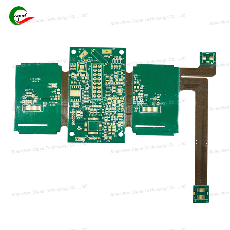
Rigid-flex PCBs mix flexible and rigid sections into one board—so their production is more involved than pure rigid or flexible PCBs. If you’re considering using them for your device (like a foldable phone or medical sensor), you might wonder: How many steps does it take to make one? And is it actually hard to produce? Let’s break this down with clear steps and plain language—no confusing factory jargon, just straight facts.
Rigid-flex PCB production builds on the steps for rigid and flexible PCBs, but adds key steps to bond the two sections. Here’s the simplified process (factories may add small tweaks, but these 6 steps are universal):
First, engineers design the PCB using software (like Altium or Eagle), marking exactly where the flexible (polyimide) and rigid (FR-4) sections will be. They also map the copper circuits, holes, and component positions.
- Next, the design is printed onto a thin, transparent “photomask film”—this acts like a stencil for the circuits.
- Why it matters: A bad design (e.g., misaligned rigid/flex sections) ruins the whole PCB later. Engineers check the design 2–3 times before moving forward.
Factories cut the base materials to size:
- Flexible layers: Thin polyimide sheets (0.1mm–0.3mm thick) with copper foil attached (for circuits).
- Rigid layers: Thick FR-4 sheets (1.6mm–3mm thick) also with copper foil.
- Then, they stack the layers in the right order: flexible layers where bending is needed, rigid layers where stability is key. A special “adhesive film” (heat-resistant, to avoid melting later) is placed between layers to bond them.
This step creates the copper circuits on both rigid and flexible layers:
- The stacked layers are coated with a light-sensitive chemical (“photoresist”).
- The photomask film is laid over the layers, and UV light is shined on top. The light hardens the photoresist only where the circuits are (as per the design).
- The unhardened photoresist is washed away, leaving exposed copper where circuits aren’t needed.
- The exposed copper is etched off with acid, leaving only the desired circuits on both rigid and flexible sections.
This is the step that makes rigid-flex PCBs unique—bonding the rigid and flexible layers into one board:

Like all PCBs, rigid-flex PCBs need holes for two reasons:
- Component holes: Small holes (0.4mm–1mm) where components (like chips or resistors) will be soldered.
- Via holes: Tiny holes (0.1mm–0.3mm) that connect circuits across different layers (e.g., a circuit on the top rigid layer to a circuit on the bottom flexible layer).
- Factories use CNC drills with camera alignment to drill holes—precision is key (a 0.1mm off drill breaks the circuit).
Finally, the PCB gets a protective coating and rigorous testing:
- Solder mask: A thin, heat-resistant coating (usually green, black, or clear) is applied to cover the copper circuits—this prevents short circuits and protects against dust/moisture.
- Silkscreen: A layer of ink is printed on top to label components (e.g., “R1” for resistor 1) for easy assembly.
- Testing: The PCB is tested for:
- Circuit continuity (do signals flow correctly?);
- Bend resistance (does the flexible section bend 10,000+ times without breaking?);
- Bond strength (do rigid/flex sections stay bonded under pressure?).
- Failed PCBs are discarded—only 90–95% pass (vs. 95–98% for pure rigid PCBs).
Rigid-flex PCBs are harder to make than pure rigid or flexible PCBs—here are the three biggest challenges that make production tricky:
If the heat, pressure, or time during bonding is off by even a little:
- Too much heat melts the flexible polyimide;
- Too little pressure leaves gaps between layers (the PCB splits when bent);
- Too long bonding makes the PCB brittle.
- Factories need specialized equipment (precision presses with temperature sensors) and trained operators—mistakes here ruin the entire batch.
Rigid-flex PCBs have both thick rigid layers and thin flexible layers—drilling through both without damaging the flexible section is hard:
- Drilling too fast melts the flexible polyimide;
- Drilling too slow leaves rough holes (components won’t fit);
- The drill bit can tilt when moving from rigid to flexible layers (causing crooked holes that break circuits).
- Even with CNC drills, 5–10% of drilled PCBs fail this step (vs. 2–3% for pure rigid PCBs).
Pure rigid PCBs only need circuit tests—rigid-flex PCBs need extra tests for flexibility and bond strength:
- Bend testing: A machine bends the flexible section 10,000–100,000 times—any crack in the bond or circuit fails the test.
- Thermal cycling: The PCB is heated to 120°C and cooled to -40°C repeatedly (500+ cycles) to check if bonding holds—extreme temperatures weaken poor bonds.
- These tests add time and cost—pure rigid PCB testing takes 1–2 hours; rigid-flex testing takes 4–6 hours.
While production is harder, rigid-flex PCBs are worth it for devices that need both bending and stability:
- Worth it if: Your device is foldable (e.g., foldable phones), has moving parts (e.g., laptop hinges), or needs to fit in tight spaces (e.g., wireless earbuds). The seamless design cuts parts and assembly time, even with higher production costs.
- Not worth it if: Your device doesn’t need bending (e.g., a TV remote) or is super low-cost (e.g., a disposable sensor). Pure rigid or flexible PCBs are cheaper and easier to make.
Rigid-flex PCB production takes 6 core steps, with extra complexity in bonding, drilling, and testing. It’s harder than making pure rigid or flexible PCBs, but factories with the right equipment and expertise handle it reliably. The key question isn’t “Is it hard?” but “Does my device need the benefits of rigid-flex?” If yes, the extra production effort pays off in a more durable, compact device.
related link:
