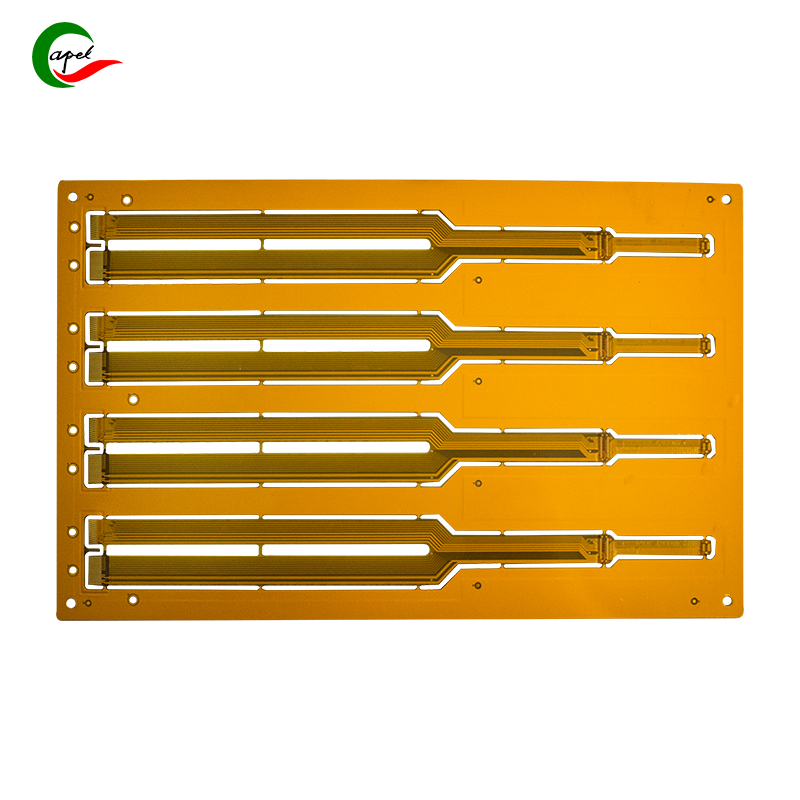
How to Choose Flexible Printed Circuit Boards (FPCB)
Date: 2025-12-01
The price of Flexible Printed Circuit Boards (FPCB) is driven by three core factors: material cost, process complexity, and production scale. The industry typically prices FPCBs by "RMB yuan per square meter" or "RMB yuan per piece," with detailed breakdowns as follows:
- Base Film:
- Polyimide (PI) base film: ~80-150 RMB yuan/㎡ (significant variation by temperature resistance; e.g., standard PI withstands -55℃~125℃, while high-end modified PI resists over 200℃ at >200 RMB yuan/㎡).
- Polyester (PET) base film: Only 30-50 RMB yuan/㎡, with a 3-5x cost gap compared to PI.
- Conductor Layer:
- Rolled Annealed Copper (RACu): ~120-180 RMB yuan/kg (high flexibility for dynamic bending), 50%-100% more expensive than Electrodeposited Copper (EDCu: 60-90 RMB yuan/kg).
- Cost increases by 3%-5% per 1μm increase in copper foil thickness (e.g., 18μm RACu costs 40% more than 9μm RACu).
- Auxiliary Materials:
- Adhesiveless structure (direct thermal compression bonding) costs 20%-30% more than adhesive-based structure (acrylate adhesive).
- Electroless Nickel Immersion Gold (ENIG) surface finish: ~1.2-1.8 RMB yuan/square decimeter, 3-4x higher than tin plating (0.3-0.5 RMB yuan/square decimeter).
- Layer Count:
- Single-layer FPCB: Benchmark price ~50-80 RMB yuan/㎡.
- Double-layer FPCB (with vias): 50%-80% premium.
- 4-layer FPCB (with blind/buried vias): 150%-200% premium.
- Multi-layer FPCB (≥10 layers): Over 500% premium (interlayer alignment accuracy ±3μm; each 1% yield reduction increases cost by 2%-3%).
- Wiring Precision:
- Reducing line width/line spacing from 50μm/50μm to 10μm/10μm adds an 80%-120% premium (requires LDI laser direct imaging with ≥5000dpi resolution and ≤3μm etching undercut).
- Special Processes:
- Rigid-Flex PCB (FR-4 rigid area lamination): 40%-60% premium over same-layer pure FPCB.
- Dynamic folding FPCB (≥1 million bending cycles): Requires RACu + adhesiveless structure, with over 100% premium.

The production process consists of 6 core stages, with key parameters and technical requirements as follows:
- Process Goal: Enhance adhesion between base film and conductor layer.
- Key Steps:
- PI base film: Plasma treatment (300-500W power, 10-30s duration, surface tension ≥40mN/m).
- PET base film: Corona treatment (15-25kV voltage to avoid high-temperature damage).
- Quality Requirements: No oil stains/scratches on the surface; thickness tolerance ±5% (e.g., ≤1.25μm for 25μm PI).
- Main Processes:
- Conventional: "Copper-clad base film → Photolithography → Etching".
- Precision fine-line: "Sputter deposition → Electroplating thickening".
- Key Parameters:
- Photolithography: LDI laser direct imaging (alignment accuracy ±2μm, line width uniformity ≤3μm); wet film thickness 10-20μm (ensuring post-etch line edge roughness Ra ≤1.5μm).
- Etching: Acidic copper chloride etchant (Cu²+ concentration 180-220g/L, temperature 45-55℃), etching rate 2-3μm/min, undercut ratio ≤1:1 (≤10μm undercut for 10μm line width).
- Quality Requirements: No open circuits/residual copper; adhesion ≥0.5N/mm (per IPC-TM-650 2.4.9 test standard).
- Multi-layer Lamination:
- Vacuum autoclave (180-220℃, 2-4MPa pressure, 30-60min holding time); interlayer alignment accuracy ±3μm (CCD alignment system).
- Adhesiveless FPCB: Controlled heating curve (5-10℃/min heating rate to avoid bubbles).
- Via Processing:
- Drilling: Laser drilling (50-150μm hole diameter, ±5μm position accuracy); mechanical drilling (≥200μm hole diameter for thick base films).
- Metallization: Chemical copper deposition (0.5-1μm Cu layer) → Electroplating (hole wall copper thickness ≥15μm, meeting IPC 2221 current-carrying requirements).
- Quality Requirements: Via conduction resistance ≤50mΩ; no hole breakage/voids (≥99.5% pass rate via X-ray inspection).
- ENIG: Nickel layer 3-5μm, gold layer 0.05-0.15μm (thin gold for soldering, thick gold ≥0.5μm for connectors); no corrosion after 48h salt spray test (5% NaCl).
- Tin Plating: Tin layer 5-15μm; ≥95% wetting area in solderability test (235℃ solder, 2-3s immersion).
- OSP (Organic Solderability Preservative): Film thickness 0.2-0.5μm; 6-month shelf life (room temperature dry environment).
- Process: Thermal compression bonding of cover film (PI/PET base + adhesive) to substrate (120-160℃, 1-2MPa pressure, 20-30s); opening position accuracy ±10μm (matching pads).
- Quality Requirements: No bubbles/lifting; adhesion ≥0.3N/mm; no cracking after 1000h at 125℃.
- Forming: Laser cutting (±5μm accuracy for irregular shapes); die cutting (±20μm accuracy for mass production); burr-free edges (Ra ≤5μm).
- Inspection:
- Electrical Testing: Flying probe test (100% coverage, conduction resistance ≤100mΩ, insulation resistance ≥10¹²Ω).
- Reliability Testing:
- Bending test (dynamic: 180° folding, 10 cycles/min, ≥1 million cycles; static: 0.5mm bending radius, 24h no open circuit).
- Thermal cycle test (-55℃~125℃, 100 cycles) with no performance degradation.
- Temperature Resistance: PI (short-term 260℃/10s, long-term 125℃); PET (short-term 150℃/10s, long-term 80℃).
- Mechanical Properties: Tensile strength (PI ≥150MPa, PET ≥50MPa); elongation at break (PI ≥40%, PET ≥100%); flexural modulus (PI ≥2.5GPa for dynamic scenarios).
- Electrical Properties: Dielectric constant (PI≈3.5, PET≈3.2 at 1MHz); dielectric loss tangent (PI ≤0.005, PET ≤0.01 at 1MHz); breakdown voltage ≥20kV/mm.
- Copper Foil Type:
- EDCu: Coarse grain, suitable for static scenarios; tensile strength ≥200MPa.
- RACu: Fine grain, suitable for dynamic scenarios; tensile strength ≥300MPa, elongation ≥15%.
- Thickness & Current-Carrying Capacity (per IPC 2221: ≤30A/mm² at 25℃):
- 18μm copper foil: ≤3A current for 1mm width.
- 35μm copper foil: ≤5A current for 1mm width.
- 70μm copper foil: ≤8A current for 1mm width.
- Surface Roughness: Ra ≤1.0μm (reduces signal loss for high-frequency scenarios ≥10GHz).
- Line Width/Line Spacing:
- Standard FPCB: 20μm/20μm (tolerance ±10%).
- Precision FPCB: 10μm/10μm (tolerance ±5%).
- High-end FPCB: 5μm/5μm (tolerance ±3%).
- Feature Sizes: Minimum pad diameter ≥50μm (for 01005 components); via diameter (laser drilling ≥50μm, mechanical drilling ≥200μm); pad diameter ≥ via diameter + 100μm (to avoid hole breakage).
- Bending Life: Dynamic bending (0.5mm radius, 180° folding) ≥1 million cycles (RACu + adhesiveless structure); static bending (1mm radius, fixed deformation) ≥1000h no open circuit.
- Environmental Adaptability: Insulation resistance ≥10¹¹Ω after 100 thermal cycles (-55℃/30min → 125℃/30min); conduction resistance change rate ≤10% after 1000h damp heat test (85℃/85% RH).
- Chemical Resistance: No corrosion or electrical performance degradation after 24h immersion in isopropyl alcohol/ethanol.
If you need FPCBs but are unsure how to choose, please leave your email address and message in the bottom right corner of the website. We will provide tailored recommendations based on your specific requirements.
