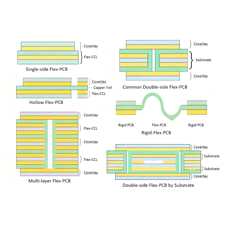
Laminated Structure of Flexible Printed Circuit Boards (FPCB)
Date: 2025-12-01
The laminated structure of Flexible Printed Circuit Boards (FPCB) is the core that enables its "flexibility, thinness, and high reliability." Laminated designs with different layer counts and material combinations directly adapt to various application scenarios (e.g., simple wiring, complex high-density, dynamic bending). Generally, the more layers an FPCB has, the stronger its performance. Below is a detailed analysis of the FPCB laminated structure from four dimensions—core component composition, key structure types (single-layer/double-layer/multi-layer), critical materials & functions, and special rigid-flex combined structure—integrated with professional parameters and application scenarios:
Whether single-layer, double-layer, or multi-layer, FPCBs are fundamentally composed of "functional layers + adhesive layers":
Lamination Structure (Top to Bottom): Cover Layer → Adhesive Layer → Conductor Layer → Base Film (Simplified version can omit the cover layer, only "Base Film + Conductor Layer + Surface Finish" for low-reliability requirements)
- Key Parameters: Line width/line spacing ≥ 100μm/100μm; total thickness 0.1-0.2mm
- Application Scenarios: Simple wiring, low-cost requirements (e.g., remote control key circuits, small sensor connecting wires, simple signal transmission for home appliances)
- Advantages: Simple process, lowest cost, best flexibility; Disadvantages: Single-sided wiring only, limited functionality, unable to achieve complex interconnection
Lamination Structure (Top to Bottom): Cover Layer → Adhesive Layer → Conductor Layer 1 → Base Film → Adhesive Layer → Conductor Layer 2 → Cover Layer
- Core Features: Interconnection between upper and lower conductor layers via "vias" (through vias, blind vias); line width/line spacing ≥ 50μm/50μm; total thickness 0.15-0.3mm
- Application Scenarios: Double-sided wiring, medium functional density (e.g., mobile phone screen connecting cables, smartwatch motherboards, small camera modules)
Advantages: More functional than single-sided FPCB, can integrate more components, maintains excellent flexibility; Disadvantages: Higher cost than single-sided FPCB, increased complexity due to via process

Lamination Structure (Typical 4-Layer Example): Cover Layer → Conductor Layer 1 → Adhesive Layer → Inner Base Film + Conductor Layer 2 → Adhesive Layer → Conductor Layer 3 → Adhesive Layer → Conductor Layer 4 → Cover Layer
- Key Components: Inner layer is "core board" (base film + conductor layer); interlayer interconnection via "buried vias" and "blind vias"; partial high-end products adopt "adhesiveless core boards" to reduce thickness
- Key Parameters: 4-20 layers; line width/line spacing ≥ 10μm/10μm (precision process up to 5μm/5μm); total thickness 0.2-0.8mm
- Application Scenarios: High-density wiring, complex function integration (e.g., hinge circuits for foldable phones, BMS (Battery Management System) for new energy vehicles, interconnection for aerospace equipment)
- Advantages: High integration, can replace multiple single/double-sided FPCBs, reducing assembly complexity; Disadvantages: Complex process (interlayer alignment accuracy ±5μm), high cost, slightly lower flexibility than single/double-sided FPCBs
- Structural Principle: On the basis of multi-layer FPCB, rigid substrates (e.g., FR-4) are embedded in local areas to form an integrated design of "flexible areas + rigid areas"
- Typical Lamination: Rigid Area (FR-4 base + thick copper conductor layer) → Transition Layer (flexible base + adhesive layer) → Flexible Area (PI base + thin copper conductor layer)
- Core Advantages: Rigid areas for component mounting and load-bearing fixation (e.g., soldering chips, connectors); flexible areas for spatial bending and dynamic connection (e.g., adapting to complex internal structures of equipment)
- Application Scenarios: Balancing stability and flexibility (e.g., mobile phone camera modules, UAV flight control boards, implantable circuits for medical devices)
- Flexibility Priority: All materials (base film, adhesive) must be flexible to avoid rigid materials affecting overall deformability
- Interlayer Consistency: Uniform thickness of each layer and even adhesive coating to prevent interlayer bubbles and peeling (which affect bending life)
- Wiring Adaptation: Use "rolled annealed copper foil" in dynamically bent areas (e.g., foldable screen hinges) to reduce copper foil fracture risk; use "electrodeposited copper foil" in static areas to lower costs
- Reliability Assurance: Cover layers must fully wrap conductor layers (except pads) to prevent oxidation; vias require metallization to enhance interconnection stability
The essence of FPCB lamination design is a balance of "material selection + layer count planning + process adaptation" — select the optimal lamination scheme based on the product's flexibility requirements, functional density, and cost budget. For example: Hinge circuits of foldable phones require "multi-layer adhesiveless FPCB + rolled annealed copper foil" to ensure a service life of millions of folds; while signal transmission for ordinary remote controls only needs "single-sided FPCB" to meet requirements.
