Date: 2026-01-28
In the world of modern electronics, where devices are constantly getting smaller and more powerful, there's a quiet hero enabling this miniaturization: the microvia. If you're designing or manufacturing today's advanced circuit boards, understanding this tiny feature is no longer optional—it's essential. Let's demystify what microvias are, why they matter, and how they're made.
What Exactly is a Microvia?
Simply put, a microvia is an incredibly small drilled hole in a PCB that connects different layers of the board. The industry formally defines it as a hole with a diameter of 150 microns (0.15mm) or less. To visualize that, it's about the width of a human hair or even finer. Unlike a standard "through-hole via" that goes through the entire board, most microvias are blind vias (connecting an outer layer to an adjacent inner layer) or buried vias (connecting inner layers only).
Why Did We Need Something So Small?
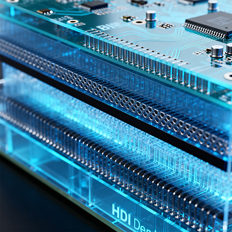
The push for microvias came from a major industry shift: High-Density Interconnect (HDI) technology. As chips got more pins with finer pitch (like modern BGAs), and boards got more layers in thinner packages, traditional drilling and routing hit a wall.
Space Saving: A single, tiny microvia takes up much less surface area ("pad size") than a standard via. This frees up precious real estate on the board for more traces and components.
Enabling Miniaturization: They are the key to routing traces out from under dense chip arrays, allowing for smaller overall board sizes.
Improved Signal Integrity: Their smaller size reduces unwanted electrical effects like inductance and capacitance, which is crucial for high-speed signals.

How Are Microvias Made? You Can't Drill Them.
This is the fascinating part. You cannot create a 100-micron hole with a mechanical drill bit—it would break. Microvias are created using a different technology:
Laser Drilling: A highly focused laser beam (usually CO2 or UV) ablates (vaporizes) a tiny portion of the dielectric material down to the next copper layer. This is a clean, precise, and fast process.
Cleaning & Preparation: The freshly created hole is cleaned of any debris.
Plating: The hole is then electroplated with copper, creating the conductive barrel that electrically connects the layers.
The Building Block Approach: Stacked and Staggered Vias
In complex HDI boards, you don't just use one microvia. They are used in advanced architectures:
Staggered Vias: Microvias on different layers are offset from each other, connected by short traces on an inner layer. This is a reliable and common method.
Stacked Vias: Microvias are placed directly on top of one another, creating a continuous conductive path through multiple layers. This is more space-efficient but also more challenging and expensive to manufacture reliably.
Important Considerations for Design and Manufacturing
While powerful, microvias introduce new factors to consider:
Cost: Laser drilling and additional process steps increase manufacturing cost compared to standard PCBs.
Reliability: The plating inside such a small hole must be perfect. Thermal stress during soldering is a key concern, as the different materials expand at different rates. Proper design and material selection (like using resin with good toughness) are critical.
Design Rules: Working with microvias requires collaboration with your PCB fabricator early on. They will specify their capabilities for minimum microvia size, pad diameters, and spacing.
In summary, the microvia is the enabling technology for the slim smartphones, powerful laptops, and advanced medical devices we use today. It represents the shift from mechanical to laser-based fabrication in PCB manufacturing, allowing engineers to pack incredible functionality into ever-shrinking spaces. When your design calls for HDI, you're calling for microvias.
Kaboer manufacturing PCBs since 2009. Professional technology and high-precision Printed Circuit Boards involved in Medical, IOT, UAV, Aviation, Automotive, Aerospace, Industrial Control, Artificial Intelligence, Consumer Electronics etc..