
Date: 2026-05-28
If you’ve ever received a brand‑new circuit board that looked more like a potato chip than a flat rectangle, you’ve seen PCB warpage. A warped board isn’t just an eyesore. It can wreck your assembly line, cause components to fall off during soldering, and turn a reliable design into a headache.
Let’s walk through what causes boards to bend, how to fix a warped PCB if it happens, and—most importantly—how to prevent warpage in the first place.
What Is PCB Warpage?
PCB warpage is exactly what it sounds like: a board that isn’t flat. Instead of lying perfectly level on a table, one or more corners lift up, or the center bows downward. Engineers classify warpage into two main types:
Bow – Uniform curvature along the length of the board. Think of a banana. All four corners touch the table, but the center rises.
Twist – A diagonal deformation. One corner lifts while the other three stay flat.
A little bit of bow or twist is normal. According to IPC standards, boards with surface‑mount components can have up to 0.75% warpage; boards without SMT parts allow up to 1.5%. However, many high‑precision assembly lines demand 0.5% or even 0.3%.
Why Does Warpage Happen?
Warpage doesn’t come out of nowhere. It’s almost always caused by uneven stress inside the board, and that stress usually comes from one of these sources.
1. Uneven Copper Distribution
This is the #1 culprit. When one area of the board has a large copper pour (like a ground plane) and another area has very little copper, those two regions expand at different rates when heated. The mismatch creates internal stress that gets locked in as the board cools. The result? A board that warps.
2. Asymmetric Layer Stackup
In a multi‑layer PCB, if the copper layers aren’t balanced – for example, thick copper on the top but thin copper on the bottom – the board will curl toward the side with more copper. This is why symmetrical stackups are so important.
3. CTE Mismatch Between Materials
Different materials expand at different rates when heated. Copper has a CTE of about 17 ppm/°C, while FR4’s z‑axis CTE is 45–55 ppm/°C. Under the intense heat of reflow soldering, these mismatched expansions create stress, and that stress often releases as warpage.
4. Rapid or Uneven Cooling
After lamination or reflow, if the board cools too quickly or unevenly, some parts shrink faster than others. Those differential shrinkage rates lock in internal stress, causing the board to bend.
5. Board Weight and Size
During reflow, most boards are supported only at the edges. Heavy components in the middle act like a weight on a trampoline, pulling the board downward and causing it to bow under its own weight.
6. V‑Cuts and Panel Design
V‑cuts are grooves that make it easy to separate individual boards from a panel. But those grooves also weaken the board’s structure, making it much more prone to warping along the cut lines.
7. Moisture Absorption
PCB materials are hygroscopic – they absorb moisture from the air. When a moisture‑laden board hits the reflow oven, that water turns to steam and expands, creating internal pressure that can cause warping, delamination, or even “popcorning” of components.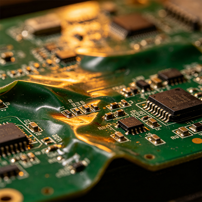
How Warpage Wrecks Your Assembly
A warped board isn’t just a cosmetic flaw. It causes real, expensive problems.
Poor component placement – Pick‑and‑place machines expect a flat surface. A warped board makes components sit crooked or miss the pads entirely.
Solder defects – Uneven contact leads to cold joints, tombstones (components standing on end), and insufficient solder wetting.
Inspection failures – Warped boards frustrate AOI machines, which rely on flat, predictable surfaces to spot defects.
Assembly line jams – In automated assembly lines, a warped board can jam a conveyor or fail to fit into fixtures, bringing production to a halt.
How to Measure Warpage
Manufacturers use a standardized test called IPC‑TM‑650 Method 2.4.22. The board is placed on a flat granite surface, and a gauge measures the maximum vertical displacement. Warpage is calculated as:
Warpage (%) = (Maximum height deviation / Board diagonal length) × 100
Can You Fix a Warped PCB?
The short answer is: probably not, especially if components are already soldered. Attempting to flatten a warped board after fabrication is an advanced process that involves reheating the board above its glass transition temperature and pressing it flat. That’s something only a factory can attempt – and even then, success is not guaranteed.
If you receive a warped bare board, your best option is usually to return it to the manufacturer for replacement. Trying to “fix” it yourself will almost certainly damage the board.
How to Prevent Warpage (Before It Starts)
Prevention is far easier than repair. Here’s what works.
At the Design Stage
Balance your copper – Distribute copper evenly across both sides of the board. If one side has large copper pours, add “dummy copper” (isolated, non‑functional copper shapes) to the opposite side to balance the surface tension.
Use a symmetric stackup – Arrange the layers so that the copper thickness and prepreg arrangement mirror each other across the center of the board.
Avoid solid copper pours where possible – Use a hatched or grid copper pattern instead of a solid pour. This reduces stress while still providing grounding and shielding.
Specify high‑Tg materials – High Tg (≥170°C) FR4 stays stiffer at reflow temperatures, reducing the risk of warpage.
Reduce panel size – Smaller panels are less likely to sag under their own weight during reflow.
Optimize V‑cut design – Keep V‑cuts shallow and away from sensitive areas to minimize structural weakness.
At the Manufacturing Stage
Pre‑bake laminates – Baking copper‑clad laminates before fabrication removes moisture and relieves internal stress, significantly reducing warpage risk.
Control cooling rates – After lamination or reflow, cool the boards slowly and evenly to avoid locking in thermal stress.
Use reflow fixtures – For especially thin or large boards, a support fixture (reflow carrier tray) holds the board flat during soldering.
At the Assembly Stage
Bake boards before reflow – A low‑temperature bake (around 105–120°C for a few hours) drives out absorbed moisture, preventing steam‑related warping during soldering.
Lower the reflow profile – Reducing peak temperatures or slowing down ramp rates can reduce thermal stress. However, be careful – this can affect solder joint quality.
Use edge supports – Don’t let heavy boards sag; use a carrier or edge‑rail system that supports the board from underneath.
Real‑World Example: The Warped BGA Board
A customer’s high‑density BGA board kept failing after reflow – not right away, but after a few thermal cycles. They couldn’t figure out why. Under inspection, the board had a subtle bow that hadn’t been caught by manual checks. During reflow, the bow lifted the BGA’s outer rows away from the board, creating intermittent connections. The solution? A thicker board core, symmetric copper distribution, and a high‑Tg laminate. The redesigned board stayed flat through reflow, and the failures stopped.
What We Can Do for You
We’re a custom circuit board manufacturer specializing in flexible PCBs, rigid‑flex boards, HDI high‑frequency boards, and PCBA. Our design and fabrication processes are built to prevent warpage from the start. We use rigorous material selection, symmetric stackups, balanced copper fills, and strict process controls to ensure every board meets IPC flatness standards. And if your design needs special treatment – like high‑Tg laminates or reflow fixtures – we can help.
Final Answer – What to Do with a Warped PCB
Fix it? – For most boards, you can’t. Return a warped bare board to your manufacturer for replacement. Attempting to flatten it yourself will likely cause more harm than good.
Prevent it? – Yes. Balance your copper distribution, use a symmetric stackup, specify high‑Tg materials, and control moisture during storage and baking.
Minimize it during assembly? – Use reflow carriers for thin or heavy boards, and carefully profile your reflow oven to avoid excessive thermal shock.
Warpage isn’t inevitable. With good design practices and proper manufacturing controls, you can keep your boards flat – and keep your assembly line running smoothly.

Kaboer manufacturing PCBs since 2009. Professional technology and high-precision Printed Circuit Boards involved in Medical, IOT, UAV, Aviation, Automotive, Aerospace, Industrial Control, Artificial Intelligence, Consumer Electronics etc..


 English



 Wechat
 +86 13670210335
 +86 13670210335
 E-mail