Date: 2025-12-25
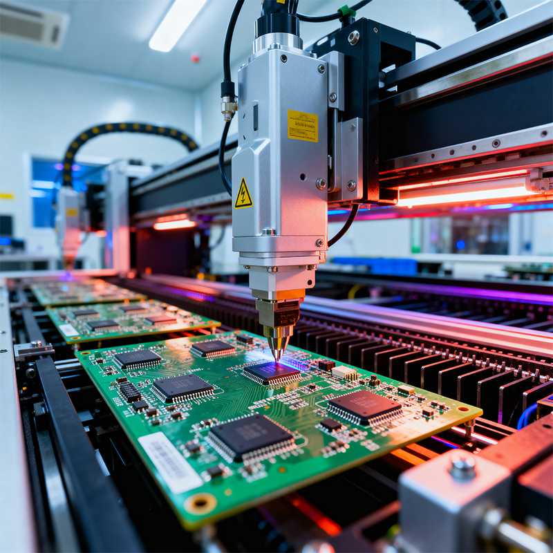
SMT PCB Board refers to a Printed Circuit Board (PCB) that is specifically designed and manufactured for assembly using Surface Mount Technology (SMT). It is the fundamental platform upon which miniature, leadless electronic components (SMDs) are mounted to create compact, high-performance electronic assemblies. Understanding this term is key to navigating modern electronics production, as it represents the dominant method for building everything from smartphones to industrial controllers.
The term combines two critical concepts in electronics manufacturing:
PCB (Printed Circuit Board): The physical board itself, made of insulating substrate (like FR-4) with laminated copper traces that form the electrical connections.
SMT (Surface Mount Technology): The assembly process where components are placed and soldered directly onto the surface of the PCB.
Therefore, an “SMT PCB Board” is essentially a PCB that is ready for or has undergone SMT assembly. Its defining features are the flat copper solder pads and fine-pitch trace designs that accommodate surface-mounted components, as opposed to boards designed primarily for through-hole components which require drilled holes.
What makes a PCB suitable for SMT? Key design and fabrication features include:
High-Density Design: Supports components on both sides, with very small trace widths and spacing (often down to 3-4 mils or less for advanced boards).
Solder Mask Defined Pads: The solder mask opening is slightly smaller than the copper pad, providing better control over solder paste deposition and reducing bridging risks.
Advanced Surface Finishes: Utilizes finishes like ENIG (Electroless Nickel Immersion Gold), ENEPIG, or Immersion Silver to ensure excellent solderability, flatness (critical for fine-pitch components), and shelf life.
Precision Registration: Layers (pads, solder mask, silkscreen) must be in perfect alignment to ensure accurate component placement by automated machines.
The transformation from a bare SMT PCB board to a functional assembly involves a highly automated, precise sequence:
1. Solder Paste Application
A stainless steel stencil is aligned over the board. Solder paste (a mix of microscopic solder spheres and flux) is printed onto the solder pads. Solder Paste Inspection (SPI) often follows to guarantee correct volume and alignment.
2. Automated Component Placement
High-speed pick-and-place machines use programmed nozzles to pick Surface Mount Devices (SMDs) from reels or trays and place them onto the pasted pads with remarkable speed and accuracy (within microns).
3. Reflow Soldering
The board travels through a multi-zone reflow oven. A carefully controlled thermal profile melts the solder paste, forming permanent, reliable electrical and mechanical solder joints as it cools.
4. Inspection, Cleaning & Testing
Automated Optical Inspection (AOI): Cameras scan the board for defects.
Cleaning: Removes flux residues (especially critical for no-clean pastes in high-reliability applications).
Testing: Electrical tests (Flying Probe, ICT) and functional validation ensure performance.
| Advantage | Impact on Your Product |
|---|---|
| Miniaturization | Enables smaller, lighter end products (wearables, mobile devices). |
| Higher Component Density | Allows more functionality in less space, supporting complex designs. |
| Superior Electrical Performance | Shorter lead paths reduce parasitic inductance/capacitance, boosting high-frequency performance. |
| Automation & Scalability | Enables fast, consistent, and cost-effective mass production. |
| Design Flexibility | Compatible with advanced board types like HDI (High-Density Interconnect) and flexible PCBs. |
Selecting the right manufacturer is crucial. Look for:
Advanced Equipment: High-precision stencil printers, multi-head pick-and-place machines, and controlled reflow ovens.
Process Expertise: Strong knowledge of solder paste management, thermal profiling, and fine-pitch assembly.
Robust Inspection: Capabilities in SPI, AOI, and X-ray for BGA and QFN components.
Supply Chain Management: Ability to reliably source a wide range of SMD components.
At Kaboer, we don’t just assemble boards; we provide a seamless bridge from your design to a reliable, high-quality SMT PCB assembly. Our owned and operated factory in Shenzhen, China gives us—and you—distinct advantages in today’s competitive market.
Your Advantage with Our Own Factory:
Direct Control & Unmatched Responsiveness: Work directly with our engineering and production teams. No middlemen mean faster communication, rapid prototyping, and agile adjustments to your project needs.
Vertical Quality Assurance: We control the entire SMT line. From solder paste storage to final inspection, our integrated quality management system ensures every batch meets stringent standards.
The Shenzhen Supply Chain Advantage: Located in the heart of the global electronics hub, we ensure efficient, cost-effective component sourcing and reduced logistics time.
Engineering Partnership: Our technical team provides proactive Design for Manufacturability (DFM) feedback, optimizing your SMT PCB design for yield, reliability, and cost before production begins.
Scalable Solutions: Whether you need 50 prototypes for NPI or 50,000 units for launch, our dedicated factory is equipped to scale with your production requirements seamlessly.
From your initial SMT PCB board design to final box-build assembly, choose a partner invested in your product’s success. Choose Kaboer for precision, transparency, and partnership.
Q1: Is “SMT PCB Board” the same as “SMD PCB”?
A: The terms are often used interchangeably, but there’s a subtle difference. SMD PCB emphasizes the components (Surface Mount Devices) on the board. SMT PCB Board emphasizes the process technology (Surface Mount Technology) used to assemble it.
Q2: Can a single PCB use both SMT and through-hole components?
A: Yes. This is called a mixed-technology board. The SMT components are assembled first via reflow soldering, followed by through-hole component insertion and a separate soldering process (like wave or selective soldering).
Q3: What are the biggest challenges in SMT assembly?
A: Key challenges include managing tombstoning (component lifting), head-in-pillow solder defects (especially with BGAs), voiding in solder joints, and achieving perfect soldering for ultra-fine-pitch or miniature components (e.g., 01005 size). These are overcome through precise process control and expert engineering.
Q4: What files do I need to provide for an SMT PCB assembly quote?
A: Essential files include:
Gerber Files (for PCB fabrication)
Bill of Materials (BOM) with specific Manufacturer Part Numbers (MPNs)
Pick-and-Place File (XYRS centroid data)
Assembly Drawings with any special instructions
Kaboer manufacturing PCBs since 2009. Professional technology and high-precision Printed Circuit Boards involved in Medical, IOT, UAV, Aviation, Automotive, Aerospace, Industrial Control, Artificial Intelligence, Consumer Electronics etc..