Date: 2026-02-04
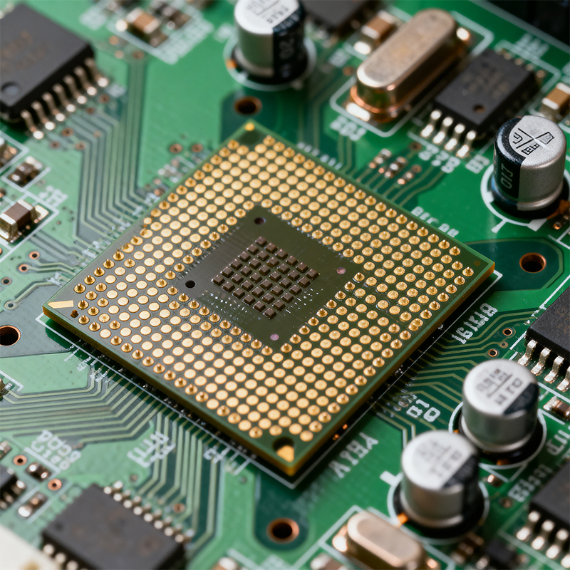
When you open up a smartphone or laptop, you might see square or rectangular chips on the motherboard whose undersides aren't lined with rows of outward-facing pins, but instead feature a grid of tiny, neatly arranged solder balls. This distinctive packaging form is the Ball Grid Array.
In simple terms, BGA is an advanced integrated circuit packaging technology that electrically connects and physically mounts a chip to an external printed circuit board. It abandons the traditional long, thin pins extending from its sides. Instead, it features hundreds or thousands of miniature solder balls arranged in a grid array on the bottom of the chip package. These balls are the "bridges" through which it communicates with the motherboard.
As processors and application-specific chips become more powerful, the number of "channels" (I/O pins) they need to exchange data with the outside world increases dramatically. Traditional perimeter-lead packaging hits its limits:
Space Constraints: Pins arranged around the perimeter are limited by the package's circumference.
Electrical Performance: Long pins introduce significant parasitic inductance and capacitance, severely impacting high-speed signal integrity.
Assembly Reliability: Thin pins are prone to bending and co-planarity issues, leading to poor solder joints.
BGA technology emerged as the solution, perfectly addressing these problems. Think of a traditional pin-lead chip as a castle with a fixed number of "drawbridges" (pins). A BGA chip is like a fortress with dense "underwater tunnels" (solder balls) covering its base—the efficiency of connection and use of internal space are fundamentally different.
A typical BGA package's core structure can be understood as a multi-layered, precision "building":
Die: The core silicon chip, connected to the next layer via extremely fine wires or flip-chip bumps.
Substrate: A miniature, multi-layer PCB with fine internal traces. It "fans out" and re-routes the dense connections from the die to the bottom ball array.
Solder Balls: The grid of tin alloy spheres (e.g., SAC alloy) on the package bottom, forming the final connection to the motherboard.
Molding Compound: The protective casing enclosing the die and internal connections.
The signal path is: Die → Redistribution within substrate traces → Bottom solder balls → Motherboard pads.
| Advantage | Explanation |
|---|---|
| High-Density Interconnect | The entire bottom area can be used for balls, providing far more I/Os (1000+) than perimeter pins in the same footprint, meeting complex chip demands. |
| Superior Electrical Performance | Extremely short connection paths drastically reduce parasitic inductance/capacitance, enabling faster, cleaner signal transmission with less noise—ideal for high-frequency, high-speed apps. |
| Better Thermal Performance | Heat from the die can be conducted directly through the solder balls to the PCB's large copper planes, offering a shorter, more efficient thermal path. |
| Higher Mechanical Reliability | Solder joints, once formed, are short and robust, typically offering better shock and thermal cycle resistance than slender pins. |
| Smaller Footprint | With no protruding pins, the board space used is essentially the package size itself, saving precious real estate. |
BGA also introduces new challenges, primarily in manufacturing and rework:
Demanding Soldering Process: Requires precisely controlled reflow soldering, with strict demands on paste printing and temperature profiles.
Inspection Difficulties: Joints are hidden beneath the chip. X-ray inspection is essential for checking solder quality (e.g., bridges, voids).
Complex Rework/Repair: Requires specialized rework stations for precise local heating to remove and replace chips, increasing difficulty and cost.
Higher PCB Design Demands: Motherboard pad layout, via fan-out design, and signal integrity control become more complex.
The BGA family continues to evolve. Common types include:
Plastic BGA: The most common, cost-effective type.
Flip-Chip BGA: The die connects directly to the substrate via bumps, offering the shortest path and best performance, used in top-tier CPUs/GPUs.
Chip-Scale BGA: Package size is nearly identical to the die size, representing the pinnacle of miniaturization.
Fine-Pitch BGA: Features smaller ball pitch (e.g., 0.5mm, 0.4mm) for higher density, posing significant manufacturing challenges.
In summary, the Ball Grid Array is a foundational packaging technology for modern high-performance, high-density electronics. By shifting connections from the "perimeter" to the "area," it fundamentally enhances a chip's interconnect capability, signal speed, and reliability. While it demands more from design and manufacturing, its immense performance benefits make BGA indispensable in everything from smartphones and computers to networking gear and AI accelerators. Understanding BGA is key to understanding the design and manufacture of today's advanced electronic products.
Kaboer manufacturing PCBs since 2009. Professional technology and high-precision Printed Circuit Boards involved in Medical, IOT, UAV, Aviation, Automotive, Aerospace, Industrial Control, Artificial Intelligence, Consumer Electronics etc..