
Date: 2026-07-17
You've definitely seen it before. A PCB covered in dense copper traces, but with a single extra wire running across the board, soldered to pads on both ends like a tiny bridge. Or maybe you've seen two closely spaced pads connected by a small blob of solder. These "extra" connections have a specific name in PCB design: a jumper.
A circuit board jumper (also called a jumper wire) is a means of creating an electrical connection between two points on a PCB [0†L11][11†L5]. It could be a piece of wire, a zero-ohm resistor, a blob of solder, or even a removable plastic cap. In this guide, I'll explain what circuit board jumpers are, what types exist, where they're used, and what to watch out for when designing them. Plain English, no fluff.
Simply put, a circuit board jumper is a "bridge" that connects two points on a PCB [0†L4-L5]. It solves one problem: what to do when copper traces can't go where you need them to go.
In multi-layer boards, traces can cross and route through different layers — there's almost always a way. But in single-sided and double-sided boards, routing space is limited. Sometimes two traces need to cross, but you can't cross them on the same layer — you need something to "jump" over [7†L6-L9]. That's where jumpers come in [7†L8-L10].
Jumpers serve two main roles: one is a planned configuration component, allowing a single board design to serve different functions [8†L7-L9]. The other is an emergency "fly wire" to fix design errors after the board is already made [11†L5-L6]. Either way, the core job of a jumper is to connect two points that can't be connected by regular copper traces [0†L18][1†L11-L12].
Circuit board jumpers come in several forms, depending on the application:
1. Wire Jumpers — The Most Flexible
A wire jumper is exactly what it sounds like — a standalone wire soldered directly to pads on the PCB [1†L11][7†L23]. It can be bare copper or insulated wire [11†L7]. According to IPC standards, bare conductor jumper wires longer than 25mm should not be used [3†L5-L7][15†L4-L6].
The advantage: simple, low-cost, and requires no PCB redesign [1†L11-L12][7†L23]. The downside: manual soldering quality directly affects reliability, and bare wires can act as antennas on high-frequency or RF paths [7†L24-L25].
2. Zero-Ohm Resistor Jumpers — The Production Favorite
A zero-ohm resistor is a surface-mount resistor with a nominal resistance of zero ohms [2†L5-L6][16†L46-L47]. It looks exactly like a regular chip resistor — same size, same pads — except it's marked "000" or "0" [16†L46-L47]. It's essentially a jumper that a pick-and-place machine can mount [6†L4-L8].
Why use a zero-ohm resistor instead of a wire? Because wires are hand-soldered; zero-ohm resistors are machine-placed [13†L28-L29]. In high-volume production, the machine places them just like any other resistor — no extra manual soldering step [6†L29-L31]. They're also easier to remove and replace than wires [6†L33-L35].
3. Solder Bridge Jumpers — The Space-Saver
A solder bridge jumper is a pair of closely spaced pads on a PCB trace that can be shorted with a small blob of solder [8†L14][1†L23-L24]. No solder = open circuit; solder bridge = closed circuit [9†L40-L41].
The biggest advantage: zero extra space and zero component cost — just two pads in the PCB layout [1†L25]. The downside: requires precise soldering control, and once bridged, it's hard to undo [7†L29-L30].
4. Header Jumpers / Shunts — User-Configurable
A header jumper is a small plastic cap with a metal spring inside that slides over two pins on the PCB [12†L20-L21]. Put it on, and the two pins are connected. Take it off, and they're disconnected [12†L23]. Computer motherboards use these for CMOS reset and hard drive master/slave settings [12†L21-L22][0†L14].
The advantage: users can change settings anytime without a soldering iron [7†L31-L32]. The downside: they take up space and can be accidentally bumped.
5. Copper Jumpers — The Ultimate
A short copper trace directly connecting two points — zero parasitic inductance, zero resistance [2†L23]. The catch? It requires layer changes or layout adjustments [2†L23].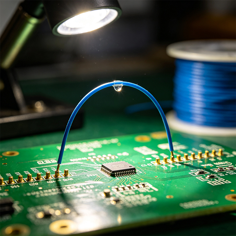
Jumpers are especially useful in these scenarios:
1. Routing Conflicts
On single- or double-sided boards, routing space is limited. When two traces need to cross and can't, a jumper lets one trace "jump" over the other [7†L33-L35].
2. Design Error Correction
You get the boards back and discover a mistake — wrong pin assignment, mislabeled silkscreen. Instead of waiting weeks and paying thousands for a new batch, a few jumpers can fix it the same day [7†L38-L41][11†L5-L6].
3. Circuit Configuration
One PCB design serves multiple product variants or regions. Jumpers let you select different configurations — solder a zero-ohm resistor for one function, leave it off for another [8†L33-L34][16†L35-L37].
4. Prototyping and Debugging
During prototyping, jumpers let you quickly test different circuit connections to validate design ideas [14†L10-L11].
Jumpers are small, but bad design causes big problems. Here are the core rules:
1. Keep Paths Short
Long jumpers introduce parasitic inductance and resistance, and can act as antennas radiating EMI [7†L42-L44]. IPC standards explicitly limit bare conductor jumper wires to no more than 25mm [3†L5-L7][15†L4-L6].
2. Keep Height Low
Jumpers shouldn't stick up too high. IPC recommends no more than 3.2mm (0.125 inches) above the board surface, or they may interfere with board mounting or suffer mechanical damage [3†L27-L28][3†L33-L35].
3. Stay Away from Sensitive Signals
Jumpers are "uncontrolled conductors" — no shielding, no controlled impedance. Keep them away from high-speed signals, RF traces, and precision analog circuits [7†L49-L51].
4. Consider Manufacturability
Zero-ohm resistors are machine-placed, making them far more production-friendly than hand-soldered wires [13†L12-L13]. If wire jumpers are used, they must be listed separately in the BOM with length, color, and preprocessing requirements [11†L8-L9]. Jumpers should follow the shortest path in the X-Y direction, and non-plated through-holes should be预留 in the PCB design if the jumper path is known in advance [11†L10].
5. Maintain Return Path Integrity
Jumper placement must not disrupt the signal return path or reference plane continuity [7†L51-L53]. Larger loop areas mean more EMI [7†L53-L54].
A circuit board jumper is a "bridge" that connects two points when regular copper traces can't. It comes in many forms: wire jumpers, zero-ohm resistors, solder bridges, header jumpers, and copper jumpers. It can be a planned configuration feature or an emergency repair.
When using jumpers, remember: keep paths short, keep height low, stay away from sensitive signals, and consider manufacturability. A well-designed jumper can save you a PCB revision. A poorly designed one can turn your board into an antenna. Next time you see an "extra" wire on a PCB — you'll know it's not a mistake. It's a jumper doing its job.

Kaboer manufacturing PCBs since 2009. Professional technology and high-precision Printed Circuit Boards involved in Medical, IOT, UAV, Aviation, Automotive, Aerospace, Industrial Control, Artificial Intelligence, Consumer Electronics etc..


 English



 Wechat
 +86 13670210335
 +86 13670210335
 E-mail