Date: 2026-02-02
Have you ever wondered why your speakers sometimes buzz when your phone receives a call nearby? Or how complex medical equipment operates reliably without interfering with each other in a hospital full of instruments? Behind the scenes, a key technology called the “PCB shield” acts as an invisible guardian inside electronic devices, ensuring different circuit modules coexist peacefully and function correctly.
In simple terms, a PCB shield is a technique and structure used to control electromagnetic interference. It has two main missions: first, to prevent sensitive signals on the board (like weak sensor readings or clear audio) from being disrupted by external “noise”; second, to stop strong internal noise sources (like high-speed processors or power modules) from affecting other components or external devices.
This invisible threat is called Electromagnetic Interference. Think of it as “noise pollution” in the circuit world. EMI is everywhere—it can come from internal sources like switching power supplies and clock signals, or from external sources like Wi-Fi routers, motors, or even lightning. Without shielding, this interference can lead to degraded performance, data errors, unstable connections, and failure to meet mandatory electromagnetic compatibility regulations in various countries.
Shielding primarily uses two physical principles to “quiet the noise”:
Reflection: Imagine blocking light with a mirror. The shield (typically metal) reflects most electromagnetic waves away, just like a mirror reflects light.
Absorption: For the portion that gets through, especially low-frequency interference, the shielding material “absorbs” its energy, converting it into minimal heat that dissipates.
An effective shield design is like a professional recording studio, utilizing both reflection and absorption to build reliable protection across the required frequency range.
Based on the scope and form of protection, PCB shielding mainly comes in these common types:
1. Board-Level Shield Can
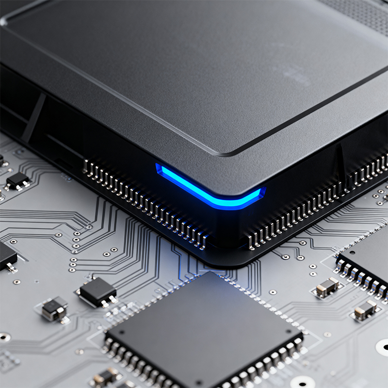
This is the classic “targeted protection.” It’s a small metal can soldered directly onto the PCB, housing and protecting a specific chipset (like a Wi-Fi/Bluetooth module or RF circuit). Its advantages are strong targeting and excellent isolation, making it common in devices like phones and routers.
2. Conductive Coatings and Films
This is a lighter, thinner “spray-on protection.” Through special processes, paints or films containing conductive particles (like silver, copper, or nickel) are coated or laminated onto the surface of the PCB or inside a plastic housing. It’s suitable for products with extreme weight and space constraints, like earbuds and smartwatches.
3. Shielded Compartments and Isolation Walls
In complex multi-layer PCB designs, layout strategies themselves can provide shielding. For example, designers might create an “isolation wall” around sensitive circuits using a ring of grounded vias, or plan separate “shielded compartments” for high-speed digital and analog areas to reduce interference from the routing stage.
Common shielding materials include highly conductive copper, cost-effective tin-plated steel, lightweight and corrosion-resistant aluminum, and highly moldable conductive plastics. Material choice involves balancing performance, cost, and manufacturability.
Designing effective shielding isn’t as simple as just adding a metal cover. Several details are critical:
Grounding is Key: The shield must be well-grounded through a low-impedance path. Otherwise, it can act like a large antenna and amplify interference.
Gaps are the Enemy: Any opening or seam in the shield is a potential leak path for electromagnetic waves. Design to minimize gaps, using conductive gaskets, finger stock, or glue for sealing when necessary.
Heat Dissipation Must Be Considered: Metal shields can trap heat. For heat-generating chips, incorporate thermal vias, openings in the shield, or thermally conductive materials to guide heat away.
In summary, PCB shielding is an indispensable part of modern, high-density, high-performance electronic devices. Though invisible, it is the unsung hero ensuring product stability, reliability, and compliance. Understanding its basic principles helps us plan this “electromagnetic defense line” from the early design stages, avoiding costly fixes later on.
Kaboer manufacturing PCBs since 2009. Professional technology and high-precision Printed Circuit Boards involved in Medical, IOT, UAV, Aviation, Automotive, Aerospace, Industrial Control, Artificial Intelligence, Consumer Electronics etc..