Date: 2026-01-30
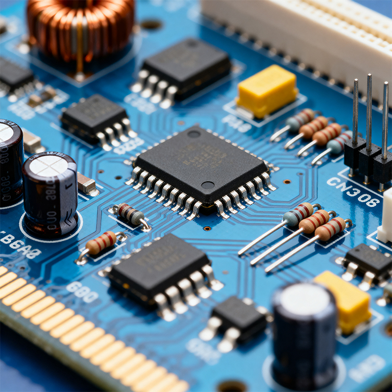
Open up any modern electronic product—a smartphone, laptop, or smartwatch—and look at the circuit board. Those tiny rectangles, cylinders, or minuscule black chips that appear to be sitting directly "on" the surface of the board are Surface Mount Components. They are the undisputed protagonists of today's electronics manufacturing world.
In simple terms, Surface Mount Components are a category of electronic parts designed for Surface Mount Technology (SMT). Unlike traditional components with long leads meant for insertion through holes, they feature flat metallized terminals (or "pads") that allow them to be placed directly onto the surface of a PCB and soldered using reflow soldering processes.
This fundamental design difference sparked a revolution in production efficiency and product performance:
| Feature | Surface Mount Components (SMD) | Traditional Through-Hole Components (THT) |
|---|---|---|
| Mounting Method | Mounted on the surface of the PCB. | Leads inserted through holes in the PCB. |
| Physical Form | Extremely small, flat, with short leads or contact pads. | Relatively larger, with long leads for insertion. |
| Assembly Density | Very high, both sides of the PCB usable, enabling extreme miniaturization. | Lower, typically assembled on one side only. |
| Production Process | Fully automated, high-speed pick-and-place, extremely efficient. | Less automated, often requires manual insertion and soldering. |
| Primary Applications | Vast majority of modern consumer electronics, communications, and medical devices. | Specific areas requiring high power, high voltage, or extreme mechanical strength. |
Categorized by function and form, SMDs come in several common package types:
Passive Components (Resistors, Capacitors, Inductors):
Rectangular Chip: Standard sizes like 0402, 0603, 0805. The numbers represent dimensions in inches (e.g., 0402 is approximately 1.0mm x 0.5mm).
Cylindrical (MELF): Offer more stable performance in some parameters.
Active Components (ICs, Transistors):
SOIC/SOP: Small Outline IC packages with "gull-wing" leads on two sides.
QFP: Quad Flat Package with leads extending from all four sides.
QFN/DFN: Quad Flat No-lead packages with thermal pads on the bottom for better heat dissipation.
BGA: Ball Grid Array. Connections are an array of solder balls underneath the chip, essential for high-density, high-performance chips.
CSP: Chip Scale Package, where the package size is close to the silicon die size.
Assembling these components onto PCBs relies on a highly automated SMT process flow:
1. Solder Paste Printing: A laser-cut stencil is used to precisely print solder paste onto the PCB pads.
2. Component Placement: High-speed pick-and-place machines accurately place components onto the paste at high speeds.
3. Reflow Soldering: The PCB passes through a reflow oven. The paste melts and cools to form reliable solder joints.
4. Inspection & Cleaning: Automated Optical Inspection (AOI) and X-Ray Inspection ensure quality. Cleaning may follow.
Choosing SMD components means choosing for your product:
Miniaturization: Enables smaller, lighter, more portable devices.
High Performance: Shorter electrical paths lead to better performance, crucial for high-speed applications.
Cost-Effectiveness & Efficiency: Ideal for large-scale, fully automated production.
However, it also introduces new design challenges: the need for precise PCB layout, stricter thermal management, and robust supply chain control.
When your design incorporates complex SMDs—especially micro packages, high-pin-count BGAs, or mixed technologies—the path from design files to a reliable finished product requires expert execution.
This is where Shenzhen Kaboer Technology provides core value. As a professional manufacturer with our own advanced PCBA factory in Shenzhen, we ensure the successful realization of your design through full-process expertise:
Deep DFM Collaboration: Our engineers provide expert DFM analysis on component selection, pad design, and layout to prevent assembly issues.
Proven Capability in Challenging Processes: We have experience handling 01005 micro-components, fine-pitch BGAs, and complex assemblies.
End-to-End Quality Assurance: From component inspection to real-time SPC monitoring and final AOI/X-Ray inspection, we implement multiple layers of quality control.
Integrated One-Stop Service: We offer a complete service from component sourcing and SMT assembly to testing. This allows you to work with a single, reliable point of contact, accelerating time to market.
Choosing Kaboer means choosing a manufacturing solutions partner that deeply understands SMT and can translate that into high-quality, reliable products.
Ready to discuss how we can bring your surface-mount design to life? Contact Kaboer today for a professional consultation.
Kaboer manufacturing PCBs since 2009. Professional technology and high-precision Printed Circuit Boards involved in Medical, IOT, UAV, Aviation, Automotive, Aerospace, Industrial Control, Artificial Intelligence, Consumer Electronics etc..