
Date: 2026-07-13
You're designing an electronic product. Maybe a smartwatch, an IoT sensor, an automotive controller, or a medical device. Your board is packed with components, space is already at the limit, and standard resistors and capacitors are down to the size of sesame seeds. What you need is a way to mount components directly onto the surface of the board — not through holes. That's a surface mount PCB.
Surface Mount Technology (SMT) is the absolute workhorse of modern electronics manufacturing — over 90% of all circuit board assemblies use SMT. The phone in your pocket, the watch on your wrist, the computer on your desk — almost every component inside them was assembled using SMT.
In this guide, I'll explain what a surface mount PCB is, how it differs from traditional through-hole technology, what its advantages are, and how the assembly process works. Plain English, no fluff.
A surface mount PCB is simply a circuit board assembled using Surface Mount Technology (SMT) . Its defining feature is simple: components are mounted directly onto the surface of the board — no holes required.
You've definitely seen the difference between the two types. In older devices, components have long metal "legs" that pass through holes in the board — these are through-hole components. On modern boards, the flat little squares sitting right on the surface are surface mount devices (SMDs).
SMDs don't have long leads. Instead, they have short terminals, pads, or solder balls. They're soldered directly onto the board's surface pads, don't take up space on the other side, and can be mounted on both sides of the board for extremely high density.
This is the most fundamental distinction in electronics manufacturing. Here's a quick comparison:
| Feature | SMT (Surface Mount) | THT (Through-Hole) |
|---|---|---|
| Mounting | Components sit on the board surface | Leads pass through holes in the board |
| Drilling | Not required | Holes must be drilled |
| Component size | Small, high-density | Large, space-consuming |
| Double-sided mounting | Yes | Usually one side only |
| Frequency capability | High-frequency (GHz capable) | Low-frequency |
| Parasitic effects | Very low | High (10-15nH inductance) |
| Mechanical strength | Moderate, needs reinforcement | Strong, ideal for vibration |
| Assembly speed | Very fast (>100k parts/hour) | Slow |
| High-volume cost | Low | High |
| Repair/Rework | Difficult (hot-air/X-ray needed) | Relatively easy |
In short: SMT makes boards smaller, faster, and cheaper. THT makes connections stronger, more vibration-resistant, and easier to hand-repair.
SMT dominates the industry for several very real reasons:
1. Smaller and Lighter
SMD components are significantly smaller than through-hole components. For the same functionality, SMT can reduce board size by 30-50%. Components can be placed on both sides of the board, maximizing space utilization. Smartphones and smartwatches keep getting smaller — that's SMT at work.
2. Faster and Cheaper
SMT assembly is fully automated — placement machines can place tens of thousands of components per hour. THT requires manual or semi-automated insertion, which is much slower. At high volume, SMT per-board costs are significantly lower than THT.
3. Better Signal Quality
SMD leads are extremely short, with parasitic inductance and capacitance an order of magnitude lower than THT. High-speed signals (USB 3.0, DDR memory, 5G RF) run cleaner and more stable on SMT boards. THT's parasitic effects severely degrade high-speed signals.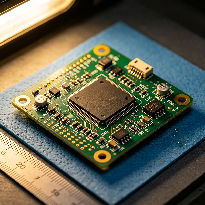
Turning a bare board into a finished assembly goes through a precise, micron-level process. One mistake and the whole batch can be scrapped.
Step 1: Data Preparation and DFM Check
The factory receives Gerber files, BOM, and pick-and-place data. First, a DFM (Design for Manufacturing) check is run — are component footprints correct? Is clearance sufficient? Are fiducials present? This step catches problems before they become physical defects.
Step 2: Solder Paste Printing
A laser-cut stainless steel stencil is placed over the PCB, and a squeegee pushes solder paste (microscopic solder spheres + flux, modern lead-free processes typically use SAC305 alloy) through the stencil openings onto each pad. Over 80% of SMT defects originate in this step. Immediately after printing, 3D SPI (Solder Paste Inspection) checks paste thickness, position, and shape.
Step 3: Pick-and-Place
High-speed placement machines use vacuum nozzles to pick components from reels and place them onto the pasted pads. Modern machines can place tens of thousands of components per hour.
Step 4: Pre-Reflow AOI
After placement and before the oven, boards go through AOI (Automated Optical Inspection) to check for missing components, misalignment, or wrong polarity. Issues can still be fixed here — once it goes in the oven, it's too late.
Step 5: Reflow Soldering
Boards enter a reflow oven with multiple heating zones. The solder paste melts ("reflows") at high temperature, forming a strong metallurgical bond between component leads and PCB pads. Then it cools and solidifies, permanently attaching the components.
Step 6: Post-Reflow AOI
Boards go through AOI again after reflow — checking for bridges, cold joints, tombstoning. For components with hidden joints (like BGAs), X-Ray inspection is required to check for internal voids.
Step 7: Testing
Finally, electrical testing — ICT (In-Circuit Test) or FCT (Functional Test). Every board is verified functional before shipping.
Bad design = bad assembly. A few critical points:
1. Pad Dimensions Must Be Precise
SMD pad dimensions must exactly match component packages. Follow IPC-7351 for land pattern design.
2. Fiducial Marks Are Required
Placement machines need fiducial marks for alignment. Add at least two fiducials on opposite corners.
3. Component Clearance Must Be Sufficient
The placement nozzle needs space. Too tight and the machine can't place components.
4. Solder Mask Dams Must Be Wide Enough
For fine-pitch components below 0.5mm pitch, solder mask dams must be wide enough to prevent bridging.
5. Large Components Need Special Attention
Large chips (BGA, QFP) need thermal vias and adequate pad support.
SMT assembly quality is governed by a complete IPC standards framework:
IPC-A-610: Electronic assembly acceptance standard — the most widely used in the world. It uses hundreds of photos and illustrations to show what acceptable solder joints look like versus defects.
IPC-7351: SMT component land pattern design standard.
IPC-J-STD-001: Soldering process requirements.
IPC-A-610 divides products into three classes:
Class 1 (General Electronics) : Function is all that matters. Toys, LED lights.
Class 2 (Dedicated Service Electronics) : Requires continuous, reliable operation. Smartphones, computers, telecom gear.
Class 3 (High-Reliability) : Aerospace, medical, military — the strictest standards.
A surface mount PCB is a circuit board assembled using SMT — components mounted directly on the board surface, no holes required.
It's smaller, faster, and has better signal quality than traditional through-hole technology — the absolute workhorse of modern electronics. SMT assembly goes through solder paste printing, pick-and-place, reflow soldering, AOI, X-Ray, ICT/FCT — a complete, precision manufacturing process. Over 90% of circuit boards use SMT.
If you're designing a high-density, compact, high-performance product, SMT is the technology you'll use. And choosing the right PCBA partner who understands SMT is how you turn your design into a reliable product.

Kaboer manufacturing PCBs since 2009. Professional technology and high-precision Printed Circuit Boards involved in Medical, IOT, UAV, Aviation, Automotive, Aerospace, Industrial Control, Artificial Intelligence, Consumer Electronics etc..


 English



 Wechat
 +86 13670210335
 +86 13670210335
 E-mail