
Date: 2025-07-11
HDI (High Density Interconnect) boards have become the go-to choice for modern electronic designs. They offer many advantages over traditional printed circuit boards (PCBs), such as higher circuit density, smaller form factors, and improved signal integrity. However, the unique design considerations of HDI boards require careful planning and execution to ensure optimum performance and reliability. Here we’ll explore the key factors that must be considered when designing an HDI board.
One of the main reasons for using HDI boards is their ability to accommodate a greater number of components in a smaller footprint. As a designer, you must consider the miniaturization aspect and carefully plan the layout of the components. Component placement plays a key role in achieving a compact design without compromising signal integrity.
To optimize miniaturization, consider using smaller, more compact components. In addition, the use of surface mount technology (SMT) enables efficient component placement, reducing the overall size of the board. However, be sure to analyze thermal considerations and ensure adequate cooling mechanisms, especially for high power components.
HDI boards support high frequency and high speed applications, so signal integrity becomes a critical consideration. Minimizing signal loss and interference is critical in order to maintain signal integrity. Here are some key factors to keep in mind:
a. Impedance Control: Ensures proper impedance matching across the board. This can be achieved by careful selection of trace width, spacing and dielectric material. Adherence to controlled impedance standards specific to your application is critical to minimizing signal attenuation.
b. Controlled crosstalk: High-density designs often result in tight trace spacing on HDI boards, which leads to crosstalk. Crosstalk occurs when a signal interferes with adjacent traces, causing signal attenuation. To mitigate the effects of crosstalk, employ techniques such as differential pair routing, shielding, and proper ground plane assignments.
c. Power Integrity: Maintaining a stable power distribution across the board is critical for optimal signal transmission. Include sufficient decoupling capacitors, ground planes, and power planes to ensure a low impedance path for power transfer.
d. EMI/EMC Considerations: As circuit density increases, so does the risk of Electromagnetic Interference (EMI) and Electromagnetic Compatibility (EMC) issues. Pay attention to proper grounding techniques, shielding strategies, and EMI filters to minimize the susceptibility of the HDI board to external electromagnetic interference.
Designing and manufacturing HDI boards can present various challenges due to increased complexity. Selecting the proper materials and fabrication techniques is critical to the success of the design. Consider the following:
a. Layer stack-up and via planning: HDI boards often have multiple layers, often in complex stack-ups. Carefully plan the layer stack-up to accommodate the desired routing density, taking into account factors such as drill size, via type (such as blind, buried, or microvia), and its placement. Proper via planning ensures efficient signal routing without compromising reliability.
b. Material Selection: Select the appropriate laminate material based on desired electrical performance, thermal management requirements, and cost considerations. HDI boards typically rely on specialized materials with high glass transition temperatures, low dissipation factors, and good thermal conductivity. Consult material suppliers to determine the most suitable option.
c. Manufacturing Tolerances: The miniaturization and increased complexity of HDI boards requires tighter manufacturing tolerances. Be sure to define and communicate your specific tolerances to the manufacturer to ensure accurate production and fit.
The reliability of an HDI board is critical to its intended application. To improve reliability and simplify troubleshooting, consider the following design considerations:
a. Design for Testability (DFT): Incorporating test points, such as logic analyzer access points or boundary-scan test points, can aid in post-manufacturing testing and debugging.
b. Thermal considerations: Since HDI boards typically pack a large number of components in a small space, thermal management becomes critical. Implement proper cooling techniques, such as heat sinks or thermal vias, to ensure that components operate within specified temperature limits.
c. Environmental Factors: Understand the environmental conditions under which the HDI board will operate and design accordingly. Factors such as temperature extremes, humidity, dust, and vibration are taken into consideration to ensure that the board can withstand its intended environment.
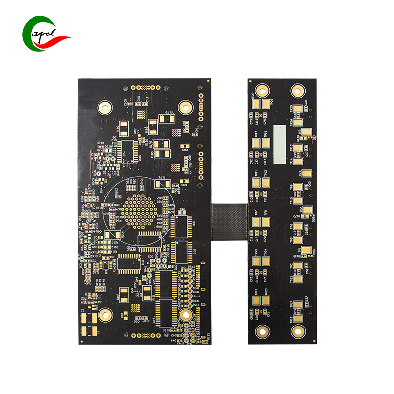
In summary, designing an HDI board requires consideration of several key factors to achieve high circuit density, optimize signal integrity, ensure reliability, and simplify manufacturing. By carefully planning and implementing a miniaturization strategy, considering signal integrity and transmission principles, selecting appropriate materials, and addressing reliability issues, you can realize the full potential of HDI technology in your designs. Shenzhen Capel Technology Co., Ltd. has been deeply involved in circuit boards for 15 years. With rigorous process flow, advanced process capabilities, professional technical services, rich project experience and innovative technology, we have won the trust of customers. And every time we can get the market opportunity for the customer’s project.
![]()
Capel manufacturing PCBs since 2009. Professional technology and high-precision Printed Circuit Boards involved in Medical, IOT, UAV, Aviation, Automotive, Aerospace, Industrial Control, Artificial Intelligence, Consumer Electronics etc..


 English


 Wechat
 +86 13670210335
 +86 13670210335
 E-mail