Discover the critical role of proper layout and routing in determining the performance and functionality of 4-layer flexible printed circuits (FPCs). Gain valuable insights into the fundamental princi……
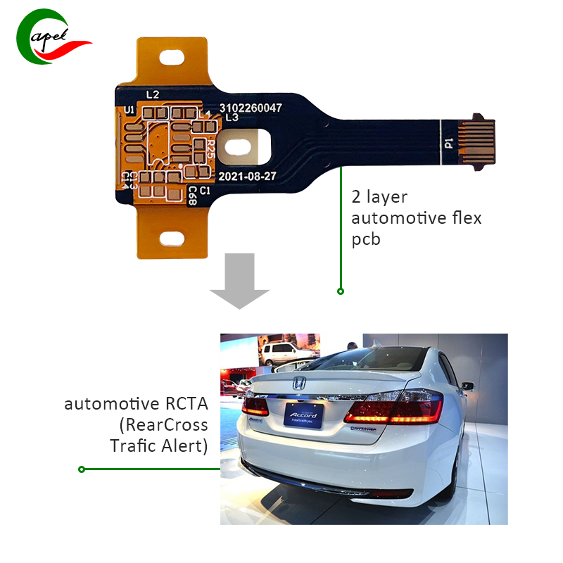
Explore the complexities of flexible PCB prototyping and manufacturing for automotive applications with a case study of a 2-layer flexible printed circuit designed for an automotive shift knob. Delve ……
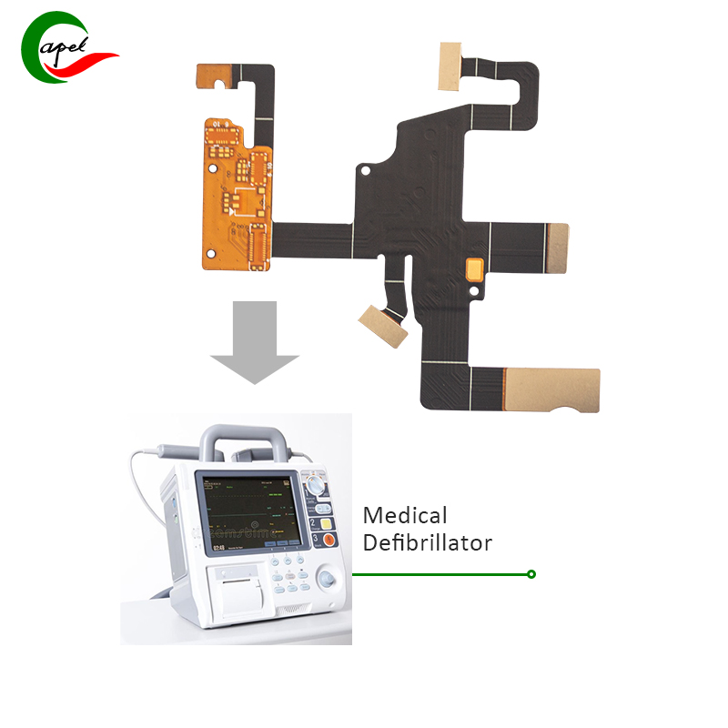
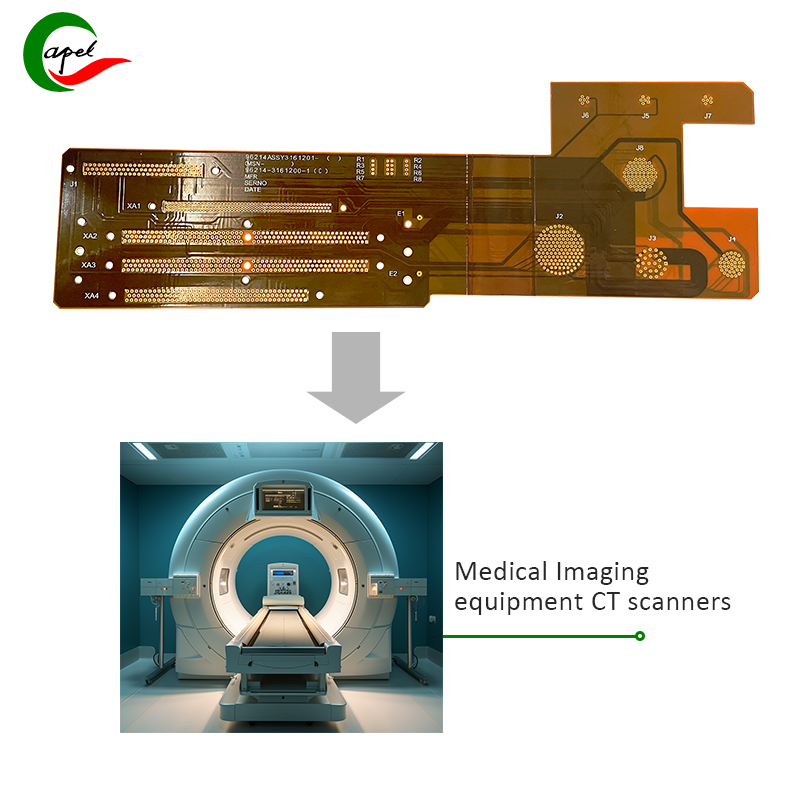
This article explores the prototyping and manufacturing process ofmedical flexible PCBs, highlighting successful case studies from the medical industry. Learn about the complex challenges and innovati……
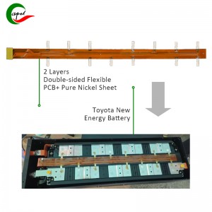
Discover how Kaboer’s advanced FPC-Flex PCB manufacturing technology meets the challenge of producing2-layer Flex PCBs for new energy vehiclebattery protection circuit boards. Dive into the technical ……
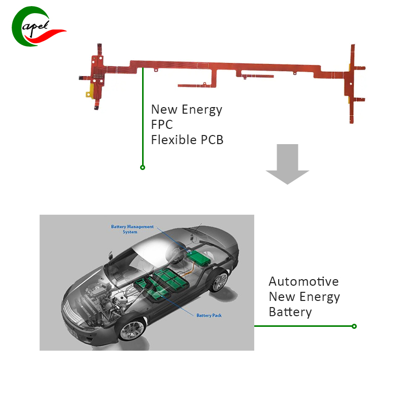
Explore Kaboer’s expertise innew energy FPCflexible PCB design for automotive applications. Get an in-depth look at their technical specifications, materials expertise and surface treatments, highligh……
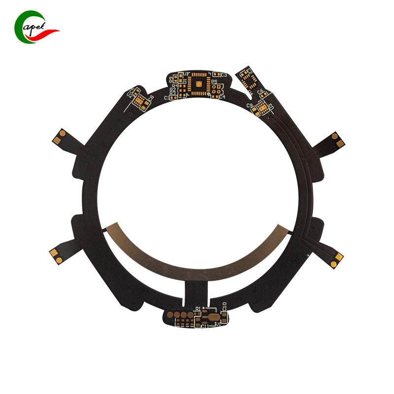
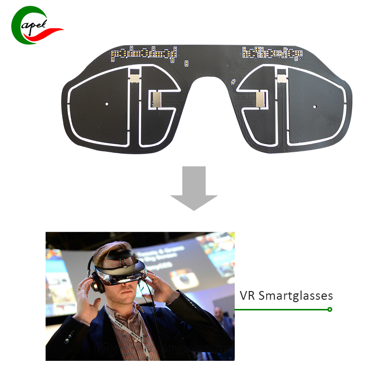
Introduce The emergence of the Internet of Things (IoT) and wearable devices has revolutionized the way we interact with technology. At the heart of these innovative devices lies the 4-layer flexib……
Chapter 1: Introduction: Get an in-depth look at the world ofmedical FPC PCBmanufacturing and the complex process of integrating FPC technology into next-generation medical devices, as discussed by……
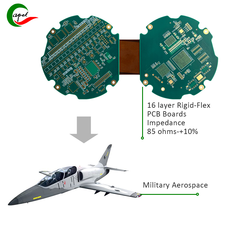
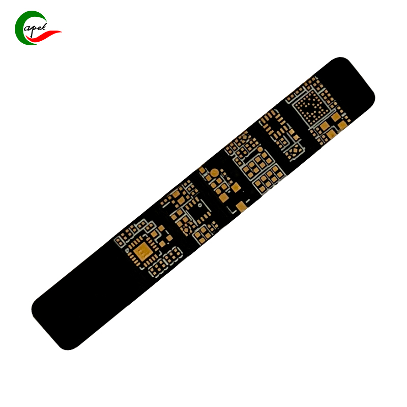
Explore the importance of 16-layer flexible printed circuits (FPC) in meeting the complex needs of the aerospace and defense industry. Learn about this technology, its applications, and the advantages……
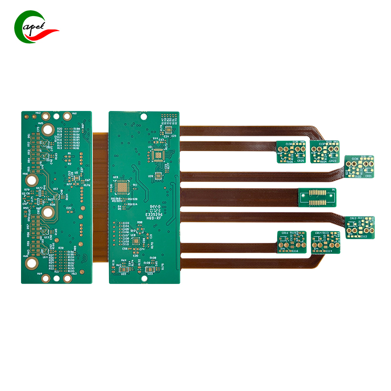
Introduce Understand the importance of 6-layer FPC (Flexible Printed Circuit) in modern electronics and its key role in various applications. Explore the intricacies of 6-layer FPC prototyping and ……
Introduction Explore the key elements of4-layer FPCflexible PCB design and prototyping in this comprehensive guide. Gain insight into the best practices, prototyping challenges, and manufacturingpr……
Flexible printed circuit boards are being actively considered for applications in extreme temperature environments. Our 2-layer flexible printed circuit boards are favored by various industries for th……
Introduction Flexible printed circuit boards (FPCs) are revolutionizing the electronics industry, offering unparalleled flexibility and design possibilities. As the demand for more compact and ligh……


 English


 Wechat
 +86 13670210335
 +86 13670210335
 E-mail