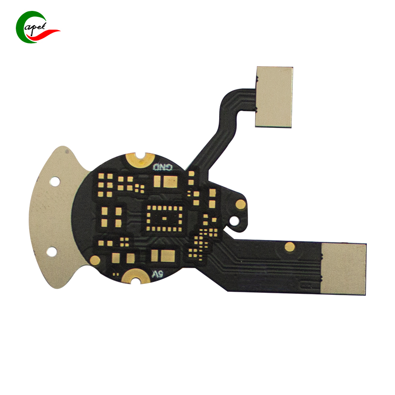
From the foldable screen on your smartphone to the sensors in a medical wearable, flexible printed circuits (FPCs) are the invisible workhorses enabling today’s most innovative devices. Their ability to bend, twist, and fit into tight spaces has made them indispensable—but not all FPCs are created equal. Understanding the different types of flexible PCBs and the processes that make them tick is key to choosing the right solution for your project. Let’s break it down.
Flexible PCBs come in various configurations, each tailored to specific needs. Here’s how they stack up:
The most basic design: a single layer of conductive copper bonded to a flexible substrate (usually polyimide, or PI).
- How they work: Copper is etched into traces to carry signals, with no extra layers or vias (holes connecting layers).
- Best for: Simple, low-cost applications like keypad connectors, camera flex cables, or basic sensor links.
- Pros: Ultra-thin (as thin as 0.05mm), highly flexible, and easy to mass-produce.
- Cons: Limited routing space—no room for complex circuits or high-density components.
Add a second layer of copper, connected by plated-through vias (PTHs) to enable more complex routing.
- How they work: Two copper layers are separated by a thin PI insulator. Vias (small holes) are drilled and plated with copper to link the layers electrically.
- Best for: Devices needing more functionality in a compact space, like smartphone display ribbons or GPS module connectors.
- Pros: More routing flexibility than single-layer designs, while retaining good flexibility.
- Cons: Slightly thicker (0.1–0.2mm) and more expensive than single-layer options.
3+ layers of copper, stacked with insulating PI layers and connected by vias. Think of them as 3D puzzles for electrons.
- How they work: Layers are bonded together under heat and pressure, with blind vias (connecting surface layers to inner layers) or buried vias (connecting inner layers only) for dense routing.
- Best for: High-performance devices like foldable phone hinges, drone flight controllers, or advanced medical monitors.
- Pros: Can handle high-speed signals, complex circuits, and even embedded components (like resistors or capacitors).
- Cons: Reduced flexibility compared to single/double-layer designs; higher production costs.
The hybrid workhorse: combines flexible PCB sections with rigid FR-4 (fiberglass) sections in one board.
- How they work: Flexible segments (often multi-layer) connect rigid areas, which host components like chips or connectors. The rigid parts add stability for soldering, while the flex parts allow bending.
- Best for: Devices needing both durability and adaptability—automotive sensors, aerospace electronics, or portable medical devices (like insulin pumps).
- Pros: Eliminates the need for connectors (which can fail), reduces weight, and simplifies assembly.
- Cons: More complex to design and manufacture; higher upfront costs.

Turning raw materials into a functional FPC requires precision engineering. Here’s a step-by-step look at the core processes:
FPCs start with a flexible substrate—almost always PI (polyimide) for its heat resistance (-269°C to 400°C) and durability.
- Why PI? It withstands soldering heat, resists chemicals, and stays flexible even after thousands of bends. Cheaper alternatives like PET (polyester) are used for low-temperature, low-stress applications (e.g., toys).
- Bonding copper: Copper foil (either electrolytic for cost or rolled for better flexibility) is bonded to PI—either with adhesive or via "adhesiveless" lamination (for higher performance, no glue means fewer defects).
This step turns a solid copper sheet into precise circuit traces.
- Photoresist application: A light-sensitive material (photoresist) is applied to the copper—either as a dry film (laminated under heat) or liquid (spin-coated for finer lines).
- Exposure: A laser or UV light projects the circuit design onto the photoresist, hardening the areas that will become traces.
- Developing: Unhardened photoresist is washed away, leaving a "mask" that protects the desired copper.
- Etching: Acid (like cupric chloride) eats away the unprotected copper, leaving only the traces. The remaining photoresist is stripped off.
Multi-layer FPCs require bonding layers together:
- Alignment: Layers are precisely aligned (within ±5μm) using tooling holes to avoid short circuits.
- Pressing: Layers are bonded under high heat (180–220°C) and pressure (10–20 kg/cm²) to fuse the PI and copper without wrinkling.
Vias (holes) are drilled to connect layers, then made conductive:
- Drilling: Laser drilling (for tiny vias, <100μm) or mechanical drilling (for larger ones) creates holes through layers.
- Plating: A thin layer of copper is chemically deposited (electroless plating) inside the vias, followed by electrolytic plating to thicken it—ensuring reliable electrical connections.
Unprotected copper oxidizes, so a finish is applied:
- ENIG (Electroless Nickel Immersion Gold): A thin gold layer (0.1–0.5μm) over nickel, ideal for high-reliability applications (automotive, aerospace) due to its corrosion resistance.
- Tin plating: Cost-effective, good for soldering, but less durable than gold.
- OSP (Organic Solderability Preservative): A thin organic film that protects copper and burns off during soldering—popular for consumer electronics.
- Coverlay: A PI film with adhesive is applied over the circuit (with openings for solder pads) to protect traces from moisture, dust, and abrasion.
- Reinforcement: Stiffeners (FR-4, stainless steel) are added to areas like connectors to prevent bending-induced damage during plugging/unplugging.
- AOI (Automated Optical Inspection): Cameras check for defects like short circuits, missing traces, or uneven plating.
- Electrical testing: Probes verify conductivity and resistance across all traces.
- Laser cutting: The FPC is trimmed to its final shape—lasers ensure precision, even for complex curves.
The type of FPC and its manufacturing process directly impact performance. For example:
- A single-layer FPC works for a simple sensor, but a foldable phone needs a multi-layer rigid-flex design with rolled copper (for 100,000+ bends).
- High-frequency 5G devices require LCP substrates and ENIG finishes to avoid signal loss.
By understanding these options, engineers can balance cost, flexibility, and performance—ensuring their device doesn’t just work, but thrives in real-world conditions.
As devices get smaller, smarter, and more flexible (think stretchable electronics or implantable medical sensors), FPC technology will keep evolving. New materials (like graphene-reinforced PI) and processes (3D-printed circuits) are already pushing boundaries.
Whether you’re designing a smartwatch or a Mars rover component, the right flexible PCB isn’t just a part—it’s the key to unlocking innovation.
Founded in 2009, our company has deep roots in the production of various circuit boards. We are dedicated to laying a solid electronic foundation and providing key support for the development of diverse industries.
Whether you are engaged in electronic manufacturing, smart device R&D, or any other field with circuit board needs, feel free to reach out to us via email at sales06@kbefpc.com. We look forward to addressing your inquiries, customizing solutions, and sincerely invite partners from all sectors to consult and collaborate, exploring new possibilities in the industry together.
