Date: 2026-01-15
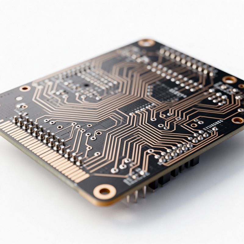
When you hold a circuit board that's completely bare—with only copper traces and pads, no components in sight—you're looking at what the industry calls a "bare board." It's like a blank canvas before the painter, or foundation plans in an architect's hands—seemingly simple, yet holding the secrets to a product's entire performance.
A bare board is the most basic form of a printed circuit board (PCB)—a board that has all its circuitry manufactured but hasn't yet received any electronic components. It consists of insulating substrate, conductive copper layers, and protective coatings, serving as both the physical skeleton and electrical pathway carrier for electronic products.
Simply put, if a fully assembled circuit board is like a furnished house, the bare board is the structural shell—walls and electrical conduits in place, just waiting for switches, lights, and appliances to be installed.
Engineers' design files (typically in Gerber format) arrive at the factory. These files act like the board's "DNA blueprint," containing precise information for every layer's circuitry.
The most common FR-4 substrate material is cut to size. This material resembles a specialized "fiberglass sandwich"—both sturdy and insulating.
One of the most precise steps. Through photolithography, the circuit pattern is transferred onto copper-clad laminate. Imagine projecting the pattern onto photosensitive material, then chemically etching away unwanted copper, leaving only the required traces.
Micro-drills create mounting holes and vias. Some holes accommodate component leads, others connect different circuit layers. Modern boards can have holes as small as 0.1mm—thinner than a human hair.
To protect copper from oxidation and ensure good solderability, bare boards receive surface treatment. Common options include:
HASL (Hot Air Solder Leveling): Traditional and economical, but with limited flatness
ENIG (Electroless Nickel Immersion Gold): Flat surface, good for fine-pitch components
Immersion Silver: Cost-effective alternative
OSP (Organic Solderability Preservative): Lowest cost option
Every bare board undergoes electrical testing to ensure no shorts, opens, or incorrect connections. This is typically done using flying probe or bed-of-nails testing.
Rigid Bare Boards: Most common type, for the vast majority of electronics
Flexible Bare Boards: Can bend and fold, for space-constrained or wearable devices
Rigid-Flex Boards: Part rigid, part flexible, balancing structural strength and routing flexibility
Single-Sided: Most basic, circuitry on one side only
Double-Sided: Circuitry on both sides, connected through vias
Multilayer: Multiple layers laminated like a pastry, for complex circuits
Metal-Core Boards: Metal backing for excellent heat dissipation
High-Frequency Boards: Special materials for stable high-frequency signal transmission
Heavy-Copper Boards: Extra-thick copper layers for high-current applications
Surface finish directly impacts subsequent soldering yield. For example, oxidized pads may cause cold joints; uneven surfaces can lead to tombstoning of small components.
For high-speed signals, bare board material properties, trace width, and spacing all affect signal quality—similar to how pipe smoothness affects water flow.
Substrate heat and moisture resistance determine board performance in harsh environments. Automotive bare boards have much stricter requirements than consumer electronics.
Seemingly simple choices about materials, processes, layer count, and size significantly affect cost. Smart bare board design can save substantial amounts in mass production.
Consumer electronics: Usually standard FR-4 double-sided or multilayer boards suffice
Automotive electronics: Require higher reliability, possibly specialty materials
Medical devices: Extremely high cleanliness and reliability requirements
Communication equipment: High-frequency performance is critical
Operating frequency? High-frequency applications need low-loss materials
Current levels? High current requires thick copper or special design
Controlled impedance needed? This affects trace design and stackup
Minimum trace width/clearance? This determines manufacturing difficulty and cost
Hole sizes and density? Affects drilling process selection
Special processes needed? Like blind/buried vias, via-in-pad, etc.
Balance these while meeting performance needs:
Material cost: Specialty materials can cost 2-10 times more
Process cost: Complex processes increase processing fees
Testing cost: High-density boards cost more to test
Actually, different board grades vary greatly in material purity, process precision, and quality control. Cheap boards may lead to hidden costs like soldering issues or early product failures.
While additional layers provide more routing space, they also increase cost, reduce yield, and may affect signal quality. If a 4-layer board solves the problem, don't use 6 layers.
Each finish has pros and cons. For example, ENIG is excellent but costly, and for some soldering processes, HASL might actually work better.
Trace widths and clearances keep shrinking—from 0.2mm to 0.1mm and below—meeting electronics miniaturization demands.
High-frequency, high-speed applications drive new material development, like lower-loss substrates and better thermal materials.
Halogen-free, recyclable materials becoming more common, with environmental concerns influencing manufacturing processes.
Increased automation, AI-assisted defect detection, making manufacturing more controllable and transparent.
Communicate with manufacturers early: Involve them during design to avoid boards that can't be manufactured or are too costly
Understand manufacturing capabilities: Know your manufacturer's limits for minimum trace width, hole size, lamination capabilities, etc.
Consider manufacturability: Avoid unnecessary complexity; simpler designs improve yield and reduce cost
Include test points: Plan for future testing and debugging—don't fill every available space
Balance ideal with practical: Find the sweet spot between ideal design and actual manufacturing capabilities/cost constraints
Bare boards are like the unsung heroes of electronics—unobtrusive yet crucial. They carry designers' creativity, determine manufacturing possibilities, and influence final product performance.
Behind every simple bare board lies crystallized materials science, precision manufacturing, and quality control. Next time you see such a "blank canvas," you might sense its potential—it's the bridge connecting idea to reality, the starting point of every electronic product.
About us: Kaboer is a PCBA company with its own manufacturing factory in Shenzhen, China. We work with bare boards of all types daily, from simple single-sided boards to complex multilayer designs. If you have questions about bare board selection or design for manufacturability, we're always happy to share practical insights from our production experience.
Kaboer manufacturing PCBs since 2009. Professional technology and high-precision Printed Circuit Boards involved in Medical, IOT, UAV, Aviation, Automotive, Aerospace, Industrial Control, Artificial Intelligence, Consumer Electronics etc..