Date: 2026-01-15
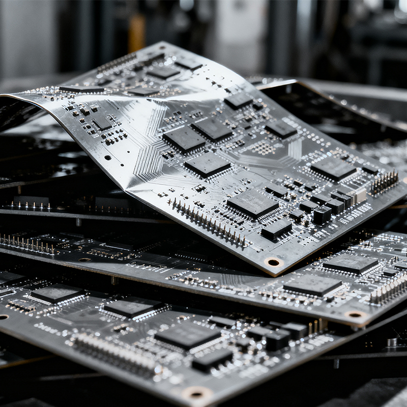
Imagine your perfectly designed circuit board looking flawless on the production line, only to come out of soldering curved like a potato chip—that's board warpage, a practical headache for many electronics manufacturers. Today, let's dive deep into this seemingly simple yet far-reaching manufacturing challenge.
Simply put, board warpage is when a circuit board loses its original flatness and develops unwanted bending. This typically occurs during manufacturing or assembly processes, especially after exposure to high temperatures.
You'll notice two main patterns:
Bow: The entire board arches gently like a bridge, with all corners lifting in the same direction
Twist: More like wringing a towel—one diagonal rises while the opposite sinks
The industry measures warpage as a percentage. IPC standards, for instance, allow up to 0.75% warpage for standard boards. That means a 30cm board could have its center 2.25mm higher than its edges.
All materials expand and contract with temperature changes, but different materials do so at different rates. Circuit boards combine multiple materials: glass-reinforced epoxy substrates, copper traces, solder mask, etc. When heated, these materials expand at different paces—like people trying to walk side-by-side with mismatched strides, inevitably pulling against each other.
A common trigger is design asymmetry. Imagine one side of a board having large copper areas (like power planes) while the opposite side has only sparse signal traces. When cooling, these sides "pull" differently, causing the board to bend toward the side with less copper.
Soldering processes, particularly reflow, heat boards above 200°C then cool them to room temperature. This rapid change stresses materials much like plunging glass into hot water then removing it.
Humidity matters too. Some board materials absorb moisture from air; when this moisture rapidly evaporates during soldering, it creates additional stress that worsens warpage.
Warped boards cause:
Component placement errors, creating shorts or opens
Uneven solder paste deposition, leading to weak joints or solder balls
Incomplete contact between BGA solder balls and pads
Modern electronics manufacturing relies heavily on automation, and machines demand flatness:
Pick-and-place nozzles may mispick components
Optical inspection systems may falsely reject boards
Boards may jam or fall off conveyor tracks
Even if initially passing tests, continuous stress from warpage can:
Accelerate solder joint fatigue, shortening product life
Potentially cause micro-cracks in internal traces
Lead to premature failure under vibration or thermal cycling
When installing boards into enclosures:
Mounting holes may misalign
Connectors may make poor contact
Reduced contact with heat sinks compromises cooling
Pursue Symmetry and Balance
Perhaps the most important design principle:
Ensure relatively even copper distribution across layers
If one side has large copper areas, try to mirror them on the opposite side
Make the stackup symmetric about the center
Optimize Material Selection
Choose materials with appropriate Tg (glass transition temperature) for your operating temperatures
Use compatible prepreg materials for multilayer laminations
Consider low-CTE (coefficient of thermal expansion) substrates
Layout Wisdom
Avoid clustering many components in one area
Replace solid copper pours with cross-hatched patterns to reduce stress
Add balancing copper features near edges and sensitive areas
Process Parameter Optimization
Control heating and cooling rates during lamination
Optimize reflow temperature profiles to avoid sharp transitions
Consider staged soldering approaches to reduce thermal shock
Storage and Handling
Maintain stable temperature and humidity in production environments
Use moisture barrier packaging, especially for humidity-sensitive materials
Avoid prolonged storage; follow "first-in, first-out" material usage
Quality Monitoring
Check flatness after critical process steps
Measure warpage using laser scanning or optical methods
Implement statistical process control to detect abnormal trends early
Correcting Minor Warpage
For slight warpage detected, consider:
Hot press leveling under controlled temperature
Adjusting assembly sequence to gradually correct through screw tightening
Using standoffs or shims to compensate for height differences
Temporary Production Line Adjustments
Modify pick-and-place machine support pin configurations
Adapt fixture designs to accommodate slight deformation
Optimize conveyor parameters to prevent jamming
Root Cause Solutions
For severe or recurring problems:
Re-evaluate material combination compatibility
Redesign for improved symmetry
Work with material suppliers to select more suitable substrates
Boards thinner than 0.8mm are naturally warp-prone and need:
Extremely strict design symmetry
Possible assembly on carrier boards
Specialized handling and processing procedures
Boards longer than 25cm may require:
Increased thickness for added stiffness
Mechanical stiffeners designed into the layout
Possible segmented manufacturing approaches
These hybrid structures need special attention:
Design smooth transitions between rigid and flexible areas
Select materials with matched expansion coefficients
Possibly specialized lamination processes
When designing or manufacturing circuit boards, ask yourself:
At design stage:
Is my stackup symmetric?
Is copper distribution balanced?
Have I selected substrates suitable for expected temperatures?
During production preparation:
Have chosen materials been compatibility tested?
Do storage conditions meet material requirements?
Have manufacturing processes been validated?
When troubleshooting:
After which process step does warpage appear?
Is it specific to certain batches or designs?
Have environmental conditions changed significantly?
Material scientists are developing:
Dimensionally more stable reinforcement materials
Resin systems with better isotropy
"Smart" materials that actively compensate for stress
Real-time warpage monitoring with automatic compensation systems
More precise temperature control systems
Big-data-based process optimization algorithms
Modern EDA tools now integrate:
Warpage prediction and simulation modules
Automatic balance checking and optimization suggestions
Material databases and selection wizards
Board warpage isn't caused by any single factor—it's the combined result of design, materials, and process. The most effective strategy is prevention at the design stage, minimizing risks through symmetric layouts and appropriate material choices.
When problems occur, analyze root causes systematically rather than just addressing symptoms. Close collaboration with material suppliers and manufacturing partners often yields the most practical solutions.
Remember, completely eliminating warpage may be unrealistic, but through scientific approaches and meticulous control, you can absolutely manage it within acceptable limits, ensuring smooth production and long-term product reliability.
Kaboer manufacturing PCBs since 2009. Professional technology and high-precision Printed Circuit Boards involved in Medical, IOT, UAV, Aviation, Automotive, Aerospace, Industrial Control, Artificial Intelligence, Consumer Electronics etc..