
Date: 2026-07-31
You're designing a new product. Maybe a wearable device, an industrial controller, a medical instrument, or an AI edge computing module. You open your design software and realize that off-the-shelf "standard boards" just won't work for what you need. You need a board with a specific shape, specific layer count, specific materials, and specific impedance — every parameter tailored to your product.
That's a custom PCB.
A custom PCB is a printed circuit board that is designed and manufactured specifically for one particular application or product. It's not a standard off-the-shelf product — its size, shape, layer count, materials, and routing are all tailored to your product. The global PCB market is expected to reach approximately $70.95 billion in 2026**, and the PCBA market is projected to hit **$103.37 billion. Behind every one of those boards is a custom PCB manufacturer.
But custom PCB manufacturing isn't just "send your files and wait." Choose the right manufacturer, and your product ships on time, on spec. Choose the wrong one, and you'll spend your days chasing deliveries, reworking defects, and arguing about responsibility. In this guide, I'll explain what custom PCBs are, what types exist, and how to choose the right manufacturing partner. Plain English, no fluff.
Standard PCB: Fixed size, fixed layer count, fixed materials — buy it off the shelf. Good for general-purpose applications like development boards and evaluation kits.
Custom PCB: Size, shape, layer count, materials, surface finish, impedance — all tailored to your product's specific requirements. Used for products that need specific shapes, high density, high performance, or specialty materials.
Simply put: A standard PCB is off-the-rack clothing — you buy it and wear it. A custom PCB is tailor-made — measured and sewn to your exact size.
The global high-layer-count PCB market was valued at $11.41 billion in 2025**, and the HDI PCB market reached **$12.88 billion — these high-value boards are almost entirely custom PCBs.
Custom PCBs aren't one-size-fits-all. Based on structure, materials, and applications, they come in several types:
1. Rigid PCB
The most common type. The substrate is FR4 fiberglass — rigid, strong, and cost-effective. Suitable for most fixed devices — industrial controllers, power supplies, appliance control boards.
2. Flexible PCB (Flex PCB)
The substrate is polyimide (PI) film — bendable. Suitable for wearables, foldable displays, printer cables, and other applications requiring bending or tight spaces. Miniaturization and high-density interconnect are key trends driving flex PCB demand.
3. Rigid-Flex PCB
Rigid and flexible sections laminated into one board. Rigid areas hold heavy chips and connectors; flexible areas handle bending connections. The global HDI rigid-flex PCB market was valued at $934 million in 2025.
4. HDI PCB (High Density Interconnect)
Trace width down to 0.05mm or less, laser blind vias down to 0.075mm or less. Supports 1-order to any-layer HDI, up to 20+ layers. Suitable for AI servers, 5G base stations, flagship smartphones, and other ultra-high-density applications.
5. High-Frequency PCB
Uses low-loss materials like Rogers, PTFE, and LCP for 5G, radar, and optical modules. The 5G PCB market was valued at $59.8 billion in 2026.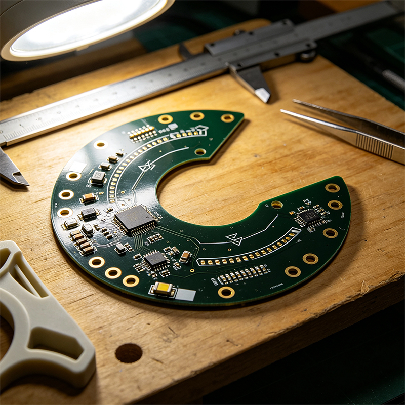
A custom PCB goes through these steps from design to delivery:
Step 1: Design File Submission
You submit Gerber files, BOM, and Pick & Place data. More manufacturers are adopting smart data formats like IPC-2581 to reduce errors during file conversion.
Step 2: DFM (Design for Manufacturing) Review
Engineers run a Design for Manufacturing check before production. In 2026, DFM is no longer a "post-design check" — it's a competitive differentiator that runs through the entire design process. DFM checks include trace width, clearance, aspect ratio, and material selection. This step catches problems before they become expensive physical defects.
Step 3: Material Preparation
Prepare substrates, copper foil, and prepreg based on your design requirements. Wrong materials mean the board won't survive its environment.
Step 4: PCB Fabrication
Includes inner layer patterning, lamination, drilling, plating, outer layer patterning, solder mask, surface finish, and testing. Multi-layer and HDI boards are far more complex than double-sided boards, typically involving over 200 process steps.
Step 5: PCBA Assembly (if needed)
If your custom board needs assembly, manufacturers provide SMT placement, through-hole assembly, inspection, and testing as a one-stop service. The trend in 2026 is turnkey services — component sourcing, PCB fabrication, assembly, and testing all under one roof.
A custom PCB's quality comes down to these metrics:
1. Impedance Control
High-speed signals (USB, PCIe, DDR, HDMI) need precise impedance control. Tolerance is typically ±10% , with high-end products requiring ±5% or better. Manufacturers must achieve target impedance through trace width, dielectric thickness, and material selection.
2. Interlayer Registration
Layers in multi-layer boards must be precisely aligned. Misregistration beyond 0.05mm means vias miss pads.
3. Aspect Ratio
Board thickness divided by hole diameter. If it's too large, plating won't reach the middle of the hole wall. Generally, keep the aspect ratio below 8:1.
4. Surface Finish
The surface finish determines solderability and shelf life. Common options include ENIG (Electroless Nickel Immersion Gold) , HASL (Hot Air Solder Leveling) , OSP, and Immersion Silver. Industrial-grade products typically choose ENIG — flat, oxidation-resistant, and long shelf life.
When choosing a custom PCB manufacturer, price is just one factor. These five dimensions are what really determine whether you'll get a good product:
Dimension 1: Manufacturing Capability
Can they actually build your board? Layer count, trace width, hole size, materials — these must match. Ask about minimum trace width, minimum hole size, maximum layer count, HDI capability, and flex capability.
Dimension 2: Quality Control and Certifications
At minimum, the factory should have ISO 9001. Automotive requires IATF 16949. Medical requires ISO 13485. IPC standard production is essential — IPC-6012 for performance, IPC-A-610 for assembly quality.
Dimension 3: DFM and Engineering Support
A good manufacturer will run a DFM check before prototyping. Issues are flagged with modification suggestions. A shop without DFM support will only discover problems after boards are made — costing you time and money.
Dimension 4: Component Sourcing Capability
If you need PCBA, ask if the manufacturer can source components for you. Experienced manufacturers have stable supply chains and can save you the hassle of RFQs, purchase orders, and logistics.
Dimension 5: Lead Time and Delivery
Sample lead time is typically 7-15 days; volume production is 15-25 days. Ask what happens if lead times are missed.
We are not a standard rigid-only PCB shop. We are a one-stop manufacturer that designs and makes flexible PCBs, rigid-flex boards, HDI high-frequency boards, and then does full PCBA.
All in-house: PCB fabrication, SMT, DIP, inspection, and assembly under one roof. From raw materials to finished boards, every step is under our control.
Full custom capability: Rigid, flex, rigid-flex, HDI, high-frequency — from simple 2-layer to 20+ layer HDI, we do it all.
High-precision manufacturing: Minimum trace/space 0.05mm, minimum laser blind via 0.075mm. Supports 1-order to any-layer HDI.
High-frequency material experience: Rogers, PTFE, LCP — for 5G and radar applications.
Flex and rigid-flex expertise: Over a decade of experience — we know how to avoid flex-to-rigid transition cracks and design proper stiffeners.
IPC-compliant: Fabrication and inspection to IPC-6012, IPC-A-610, and IPC-J-STD-001 — Class 2 and 3.
Turnkey PCBA services: Component sourcing, SMT placement, DIP insertion, AOI/X-Ray inspection, FCT testing — one window, one responsibility.
Free DFM review: Send your design files, get a DFM report within 24 hours — including trace width, clearance, aspect ratio, impedance, and material recommendations.
Three simple steps:
Send your files: Gerbers, BOM, stackup and impedance requirements, specialty material needs.
We review and quote: Within 24 hours, you'll receive a DFM report, material recommendations, and sample/volume pricing.
Sample, then scale: We build 10-20 samples. You test functionality and reliability. Then we move to volume.
Custom PCBs aren't "more expensive boards" — they're the key to making your product stand out in the market.
The global PCB market is growing at over 5% annually. AI servers, 5G base stations, autonomous driving, wearables — every product in these new sectors is powered by a custom PCB.
If you're looking for a manufacturer that truly understands custom boards, high-layer-count boards, HDI, and rigid-flex, send us your requirements. We won't push a contract — we'll first run a free DFM review and material recommendation, and let our expertise speak.
When you contact us, please include:
Product type and application
Estimated layer count and whether flex/high-frequency is required
Estimated annual quantity (samples, small batch, or mass production)
We'll give you an honest answer — what we can do, what we can't, and how to modify your design to make it work.

Kaboer manufacturing PCBs since 2009. Professional technology and high-precision Printed Circuit Boards involved in Medical, IOT, UAV, Aviation, Automotive, Aerospace, Industrial Control, Artificial Intelligence, Consumer Electronics etc..


 English



 Wechat
 +86 13670210335
 +86 13670210335
 E-mail