
Date: 2026-07-31
You're designing a high-end electronic product. Maybe an AI server, a 5G base station, an ADAS system, or a flagship smartphone. Standard PCBs don't have the routing density, signal integrity, or board space for what you need. You need an HDI PCB.
HDI stands for High Density Interconnect. It's not a specific type of board — it's a complete set of higher-density, finer-feature, more complex PCB manufacturing technologies. The global HDI PCB market was valued at approximately $12.88 billion in 2025** and is projected to reach **$17.56 billion by 2031. AI compute boards accounted for 43.4% of PCB investment in 2025 — HDI has become standard equipment in high-end electronics.
But HDI boards aren't something you can just send to any PCB shop. They require laser drilling, sequential lamination, microvias, and stacked via structures — a complete set of specialized equipment and processes. Choose the wrong manufacturer, and you'll face delayed deliveries, low yields, or a scrapped project. In this guide, I'll explain what HDI PCBs are, how they differ from standard boards, and how to choose the right manufacturing partner. Plain English, no fluff.
Here's the core difference: standard PCBs use mechanical drilling + through-holes — holes that drill all the way from top to bottom. HDI uses laser drilling + microvias and buried vias — these holes don't go all the way through, they only connect adjacent layers.
Think of HDI as "micro-sculpting" for circuit boards. Traditional through-holes pass through every layer, taking up routing space on each one. HDI microvias only connect between adjacent layers — leaving valuable routing channels open on other layers. Traces can be finer (50μm or smaller), holes can be smaller (below 100μm), and layer counts can be higher (20+ layers).
HDI manufacturing relies on three core technologies:
Laser drilling: CO₂ or UV lasers drill microvias with micron-level precision
Sequential lamination: Layers are built up one at a time, with vias drilled after each lamination cycle
Microvias and buried vias: Replace traditional through-holes to save routing space
Based on the number of laser drilling steps, HDI is classified as 1-order, 2-order, 3-order, with the highest level being Any-Layer HDI — where every layer can connect directly to adjacent layers via microvias. Flagship smartphones use Any-Layer HDI. Flagship phones now incorporate 10-14 microvia layers to route mmWave antenna arrays and multi-camera modules.
| Feature | Standard PCB | HDI PCB |
|---|---|---|
| Drilling | Mechanical drilling | Laser drilling primarily |
| Via types | Through-holes | Blind, buried, microvias |
| Min trace width | ≥50μm | Down to 25μm or less |
| Min hole size | ~0.15mm | 75μm or less |
| Layer count | Any | Typically 8-20+ layers |
| Signal quality | Moderate | Excellent |
| Best for | General products | AI servers, 5G, ADAS, flagship phones |
HDI's core value: pack more circuitry into less space while maintaining signal integrity at high speeds. As chip packages shrink and signal rates climb, standard PCBs simply can't keep up.
HDI is used wherever "standard boards can't handle it":
AI Servers and High-Performance Computing: AI compute boards accounted for 43.4% of PCB investment in 2025. AI chips need extreme routing density and signal integrity — HDI is the only choice.
5G Communications: 5G base stations and mmWave antennas need low-loss, high-frequency PCBs. HDI's fine lines and microvias minimize signal attenuation at high frequencies.
ADAS and Autonomous Driving: Advanced driver-assistance systems demand high-reliability, high-density PCBs. Automotive radar and camera modules require exceptional signal integrity.
Flagship Smartphones: Flagship phones now incorporate 10-14 microvia layers. Any-Layer HDI is standard.
Medical Devices and Aerospace: High-reliability, miniaturized devices. Medical applications demand extreme reliability and compact form factors.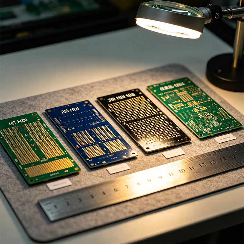
HDI PCBs aren't "standard PCBs with a few extra steps" — they require completely different equipment and processes. When evaluating an HDI PCB manufacturer, focus on these areas:
1. Laser Drilling Capability
The core of HDI is the microvia. Manufacturers must have CO₂ or UV laser drilling systems with hole diameter control within ±5μm. If they can't laser-drill, they can't make HDI.
2. Sequential Lamination Capability
HDI boards are built layer by layer — each lamination cycle adds a layer, drills vias, and patterns circuits. Advanced manufacturers handle six or more lamination cycles. Interlayer alignment precision directly determines yield — misregistration beyond 0.05mm means vias miss pads.
3. Fine-Line Capability
HDI trace/space is typically 75μm/75μm or finer. High-end HDI can go down to 25μm or less. The finer the line, the higher the manufacturing difficulty and the tighter the yield control.
4. Stacked Via and Via-in-Pad Capability
High-order HDI requires stacked vias — multiple microvias stacked in the same location — and via-in-pad — vias placed directly in component pads. Both require extreme precision and plating control.
5. Material and Impedance Control
HDI performance is 70% material, 30% process. High-speed/low-loss materials accounted for 42.63% of the HDI market in 2025. Manufacturers must be familiar with Megtron, NPG, PTFE, Rogers and other high-frequency low-loss materials. Impedance tolerance must be ±5% or better.
6. IPC Standards Compliance
HDI has dedicated industry standards — IPC-2226A (HDI design) and IPC-4104 (HDI materials). Reliable manufacturers should have at least ISO 9001, with IATF 16949 for automotive and ISO 13485 for medical applications.
A few common pitfalls in HDI design:
Minimum Design Rules ≠ Stable Production Capability
Many designers push to the limit — minimum trace width, minimum hole size, tightest spacing. But in HDI manufacturing, minimum design rules, even if they pass a DFM check, do not guarantee repeatable and stable production yield. Reliable production capability and "theoretically possible" are two different things. Slightly increasing clearances in critical areas and using larger capture pads can have a significant impact on yield.
Thermal Stress in Stacked Vias
Stacked via structures go through multiple high-temperature, high-pressure lamination cycles. If the material doesn't have high enough Tg or sufficient dimensional stability, microvias will crack and layers will shift out of registration. This is why high-order HDI requires high-Tg materials (180°C+).
Stackup Planning Comes First
HDI stackups are far more complex than standard boards — rigid sections, flex sections, microvia layers, buried via layers… You must define the stackup before you start routing, not after.
We are not a standard rigid-only PCB shop. We are a one-stop manufacturer that designs and makes flexible PCBs, rigid-flex boards, HDI high-frequency boards, and then does full PCBA.
Full HDI manufacturing capability: 1-order, 2-order, 3-order, Any-Layer HDI. Minimum trace/space 0.05mm, minimum laser blind via 0.075mm, up to 20+ layers.
Sequential lamination and stacked via expertise: We master sequential lamination with stacked via and via-in-pad support — ensuring interlayer alignment and microvia reliability.
High-frequency low-loss material experience: Rogers, Megtron, PTFE, LCP, high-Tg FR4 — we've done them all for 5G, AI, and automotive applications.
All in-house: PCB fabrication, SMT, DIP, inspection, and assembly under one roof. From HDI sequential lamination to assembly, every step is under our control.
SPI + AOI + X-Ray: Solder paste inspection, post-placement inspection, post-reflow inspection, BGA inspection — quality checks at every stage.
IPC-compliant: Fabrication and inspection to IPC-2226A, IPC-6012, IPC-A-610 — Class 2 and 3.
Free DFM review: Send your design files, get a DFM report within 24 hours — including stackup design, microvia layout, impedance control, and manufacturability assessment.
HDI projects we've served: AI accelerator substrates, 5G small cell boards, automotive radar high-frequency boards, flagship phone motherboards, medical endoscope rigid-flex HDI boards.
Three simple steps:
Send your files: Gerbers, BOM, stackup and impedance requirements, HDI order requirements.
We review and quote: Within 24 hours, you'll receive a DFM report, stackup recommendation, and sample/volume pricing.
Sample, then scale: We build samples. You test functionality and reliability. Then we move to volume.
HDI PCBs aren't "more expensive standard boards" — they're the solution to routing density, signal integrity, and miniaturization challenges. The global HDI market is growing at over 5% annually, and AI and 5G are turning HDI from a "high-end option" into an "industry standard."
If you're looking for a manufacturer that truly understands HDI, microvias, and high-frequency low-loss materials, send us your requirements. We won't push a contract — we'll first run a free DFM review and stackup recommendation, and let our expertise speak.
When you contact us, please include:
Product type and application (AI server, 5G, ADAS, smartphone, etc.)
Estimated layer count and HDI order requirement (1-order, 2-order, Any-Layer)
Estimated annual quantity (samples, small batch, or mass production)
We'll give you an honest answer — what we can do, what we can't, and how to modify your design to make it work.

Kaboer manufacturing PCBs since 2009. Professional technology and high-precision Printed Circuit Boards involved in Medical, IOT, UAV, Aviation, Automotive, Aerospace, Industrial Control, Artificial Intelligence, Consumer Electronics etc..


 English



 Wechat
 +86 13670210335
 +86 13670210335
 E-mail