Date: 2025-12-24
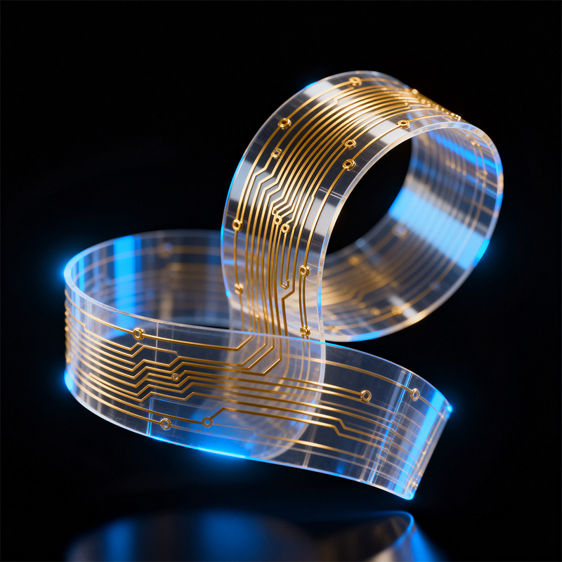
Etched FPC refers to a Flexible Printed Circuit manufactured primarily through a subtractive chemical etching process. This method precisely removes unwanted copper from a flexible substrate to create intricate conductive pathways, enabling the high-density, lightweight, and reliable interconnections essential for modern compact electronics. This guide explains the etched FPC process, its advantages, and key design considerations.
An Etched FPC is produced by laminating a thin layer of copper onto a flexible polymer film (like polyimide or PET). The desired circuit pattern is then defined using photolithography and chemically etched away, leaving behind only the precise copper traces needed. This contrasts with additive processes (like printing conductive ink) and is the industry-standard method for producing high-performance, reliable flexible circuits.
Why "Etching" is Central: The etching process determines the precision, line width/spacing, and overall fidelity of the circuit. It is the critical step that transforms a blank copper-clad laminate into a functional, high-density flexible circuit.
The manufacturing of an etched FPC involves several meticulous steps:
Material Preparation: A roll of flexible dielectric film (typically polyimide for high-temperature performance) is coated with a thin layer of copper foil.
Cleaning & Surface Treatment: The copper surface is cleaned and treated to ensure optimal adhesion for the photoresist.
Photolithography (Patterning):
A light-sensitive photoresist is applied to the copper.
The circuit design, printed on a photographic film (phototool), is placed over the resist.
UV light exposes the resist through the phototool, hardening it in the areas that will become the final circuit traces.
The unexposed (soft) resist is then developed away, revealing the copper that needs to be removed.
Chemical Etching (The Core Step): The panel is immersed in a chemical etchant solution (e.g., ferric chloride or alkaline ammonia). This solution dissolves the exposed copper, while the copper protected by the hardened photoresist remains intact.
Stripping & Cleaning: The remaining photoresist is stripped off, revealing the precise copper circuit pattern. The panel is thoroughly cleaned.
Coverlay Application & Finishing: A protective insulating layer (coverlay) is laminated over the circuit, leaving only pads exposed. Final steps include plating (e.g., ENIG for solderability), testing, and singulation.
| Feature | Etched FPC (Subtractive) | Additive/Printed FPC | Why It Matters for Manufacturers |
|---|---|---|---|
| Precision & Resolution | Extremely High. Achieves trace widths/spacing down to 25µm (1 mil) or less. | Limited. Typically >100µm (4 mil). | Enables high-density interconnects (HDI) for miniaturized devices like wearables, medical sensors, and advanced cameras. |
| Conductor Quality | Excellent. Uses solid, rolled/electrodeposited copper foil. Low resistivity, high current capacity. | Variable. Conductivity depends on ink formulation and curing. | Ensures signal integrity, reliability, and power delivery in demanding applications. |
| Durability & Reliability | Superior. Strong bond between etched copper and polyimide. Excellent flex endurance. | Can be prone to cracking; adhesion may be weaker. | Critical for dynamic flexing applications (hinges, repeated motion) and harsh environments. |
| Process Scalability | Highly Scalable. Ideal for medium to high-volume production with consistent quality. | Best suited for prototyping or very low-volume runs. | Provides cost-effectiveness and consistency for commercial production scales. |
To leverage the full potential of etched FPC technology, consider these design rules:
Minimum Trace/Space: Consult your fabricator's capabilities. Standard is 75-100µm; advanced etching can reach 25-50µm.
Copper Weight: Common weights are ½ oz (18µm) to 2 oz (70µm). Thicker copper for higher current, but limits fine-line etching.
Bend Radius: Design traces to run perpendicular to the bend axis. Specify a minimum bend radius (e.g., 6x material thickness for static, 10x for dynamic flex) to prevent cracking.
Stiffeners: Plan for localized rigid areas (using FR4 or polyimide stiffeners) for component mounting and connector insertion points.
Etching Uniformity: Account for a slight undercut during etching. Experienced manufacturers compensate for this in the phototool design.
Etched FPCs are indispensable in industries where space, weight, and reliability are paramount:
Consumer Electronics: Smartphone displays, cameras, folding phones, laptops.
Medical Devices: Hearing aids, endoscopes, wearable monitors, imaging probes.
Automotive: LED lighting arrays, infotainment systems, sensors (airbag, pressure).
Aerospace & Defense: Avionics, satellites, guidance systems (due to light weight and vibration resistance).
Industrial & Robotics: Compact sensors, moving arm interconnects, precision instruments.
Q1: What is the main difference between "etched FPC" and standard "FPC"?
A: "Etched FPC" specifically highlights the subtractive chemical etching process used to form the circuits. This is the most common and precise method for mass-producing FPCs. "FPC" is the general product category.
Q2: What are the limitations of the etching process?
A: It generates chemical waste that requires proper treatment. Very thick copper (>3 oz) is challenging to etch with fine resolution. The process is less economical for single-piece prototypes compared to additive methods.
Q3: Can etched FPCs have plated through-holes (PTH)?
A: Yes. A critical capability is forming reliable PTHs in flexible materials to create double-sided or multilayer flexible circuits, enabling more complex interconnections.
Q4: How do I choose between polyimide (PI) and PET as the base material for an etched FPC?
A: Polyimide (PI) is the standard for most applications due to its excellent high-temperature resistance (soldering), chemical stability, and flex endurance. PET (Polyester) is a lower-cost alternative suitable for simpler, non-high-temperature applications (e.g., simple membrane switches).
Kaboer manufacturing PCBs since 2009. Professional technology and high-precision Printed Circuit Boards involved in Medical, IOT, UAV, Aviation, Automotive, Aerospace, Industrial Control, Artificial Intelligence, Consumer Electronics etc..